
Samsung Electronics Co. Ltd. has opened the doors to its new Device Solutions America headquarters in San Jose, Calif., which is designed to expand the company’s R&D efforts of its semiconductor operations.
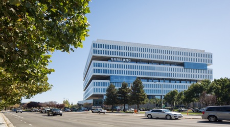 Samsung's new American-based headquarters in San Jose, Calif. Source: SamsungThe new headquarters for Samsung’s Device Solutions America is located in the same corner of Silicon Valley where Samsung’s original campus was first built more than 30 years ago. The company says that its America headquarters has always been a strategic asset to the its R&D efforts and with the opening of this new location, it will continue that tradition. The facility will help generate the next-generation of innovation and advanced technologies in the semiconductor market, the company says.
Oh-Hyun Kwon, vice chairman and CEO of Samsung Electronics, says the facility is helping Samsung to lay “the groundwork for a more aggressive pace of growth over the next several decades.”
The opening of the facility will bring together 700 employees from around Silicon Valley into a 1.1 million-square-foot facility that will house various research labs dedicated to semiconductors, light emitting diodes (LEDs) and displays.
Samsung calls the San Jose campus one of the most strategically important facilities in the U.S. and one of the biggest investments it has made in Silicon Valley.
Questions or comments on this story? Contact engineering360editors@ihs.com
Related links:
IHS Semiconductors & Components
News articles:
Apple and Samsung Can Co-Exist in Same Market
Samsung Charges Down a Different Path
