
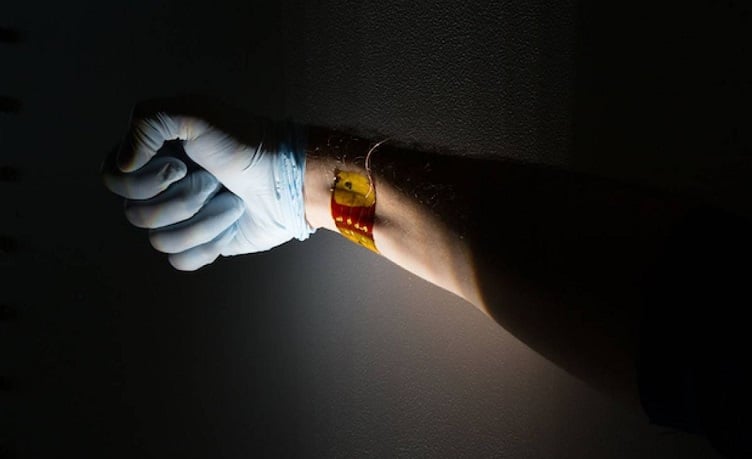
A new frontier in semiconductor research is finding ways to convert regular, stiff semiconductors into flexible chips that can be bent to conform to other geometries. The chemistry is significantly different from silicon wafers or III-IV semiconductors commonly used for modern applications. However, there are already numerous applications for this technology, and so there is a strong driving force for development in this field.
Applications of flexible semiconductors
The three biggest applications for flexible semiconductors are:
- Wearables
- Portable electronics
- Industrial internet of things (IIoT)
The nature of flexible semiconductors also makes them thinner than traditional semiconductors, reducing the thickness of an overall device, potentially opening a path toward other applications.
Wearables and biosensors
The success of fitness bands has brought wearable electronics into the mainstream marketplace. A typical fitness tracker can track the number of steps, pulse, number of stairs climbed and other parameters. More advanced ones can monitor sleep, heart rate and even the pattern of your heartbeat.
The biggest source of inaccuracy is the fact that the sensor package is not always in contact with the skin. This can lead to “phantom” step counts as it bounces around or “missing” steps or missing pulse due to the lack of contact.
Flexible semiconductors could make a major impact on this market. Instead of rigid semiconductors in a rigid plastic case, flexible semiconductors can conform to the shape of the wearer’s body. This improves contact and can collect more accurate data.
Furthermore, tight contact also means new metrics can be tracked that would otherwise be difficult. New biosensors mounted directly on the skin could measure blood oxygen content, blood glucose levels and other biomarkers in real time. Such skin patches could also be used for monitoring lactate to prevent athletes from overtraining, neural sensors for monitoring brain activity to track sleep disorders and many other specialty metrics.
New implantable devices would also be possible with flexible semiconductors. Insulin pumps, pacemakers and other electromechanical devices could be made to conform to existing tissue and bone structures, rather than being a hard object implanted next to these structures, according to the UChicago Pritzker School of Molecular Engineering.
Portable and personal electronics
Several smartphones and tablets on the market feature foldable screens. These have some limitations, as the screens fold only in certain areas. With flexible semiconductors, the screen could potentially be folded into multiple shapes, collapsing into a convenient package for transit.
Picture a screen that can be extended to the size of a laptop screen that folds up into the size of a smartphone.
Besides folding displays, flexible displays could be embedded into glasses, virtual reality headsets and other such devices. The flexibility makes them a more natural fit and more customizable to the person. One application for this is for the vision impaired who can only see a very short distance from their eyes. Using an embedded camera, the image can be projected onto the glasses, giving them much better vision overall.
Hearing aids can be made more flexible and provide a better fit for the person’s ear. Furthermore, speech recognition devices and flexible microphones can be fitted on a person’s throat to measure vibrations and produce more accurate recordings. Flexible semiconductors like microphones could be used to reduce speech impediments and amplify weak or failing voices.
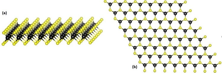 TMDC structure. (a) a side view and (b) a top view, where the black atoms are the metal atoms and the yellow are the chalcogen atoms. Source: Wikipedia.
Industrial IoT
Just like the other markets, flexible sensors and flexible arrays make it possible to fit in new places and make more accurate measurements.
Consider a network of pipes in a chemical processing plant. Instead of just labeling the pipes, a small, flexible sensor network could be fitted to the pipe and feed a flexible display with information like chemical name, flow rate, pressure and temperature, all without drastically increasing the footprint of the pipe network.
In robotics, soft grippers can be outfitted with sensors that can measure the pressure on the grips. As a feedback loop, the sensor can measure the pressure and then activate a soft actuator that tightens or loosens the grip. This system is much more efficient than measuring the pressure behind the soft grips.
Flexible solar cells can be wrapped to conform to existing structures. Instead of the need for a heavy metal rectangular frame, thin, flexible solar panels could be placed on existing siding, water towers and other surfaces that represent valuable space. At the private level, this means there will be more possibilities for solar energy. At the municipal level, spaces already dedicated to infrastructure can serve a secondary role generating electricity.
Flexible semiconductor chemistry
While there are numerous ways to use flexible semiconductors, what makes a flexible semiconductor? Silicon, gallium arsenide and other commonly used semiconductors are brittle and will not bend. Instead, transition metal dichalcogenides (TMDCs) have been the major focus of flexible semiconductor research. These materials take on the form of MX2, where M is the transition metal (such as molybdenum) and X is a chalcogen, such as sulfur. The metal is sandwiched between the chalcogen atoms and can be only a few thin atoms.
These materials exhibit semiconductor properties, just like silicon. However, unlike silicon, they are also lightweight, stretchable and flexible, making them ideal for making wearables, and other soft items that need to conform to organic shapes.
Poly(3-hexylthiophene) (P3HT) is another common flexible semiconductor. It is used in flexible solar cells and will see more applications in the future.
Manufacturing techniques
The manufacture of flexible semiconductors is far from trivial. However, recent developments in “foundry” semiconductor work have made their creation possible.
Constructing and operating a semiconductor cleanroom is not a trivial undertaking. For years, companies would sell the rights to new designs to the larger semiconductor manufacturers instead of trying to perform the manufacturing in-house. Due to the economy of scale, many innovative designs were simply not developed as it was not cost effective to build a cleanroom nor sell the design.
In recent years, there has been an uptick in “foundry” work. Semiconductor foundry work is similar to foundry jobbing work in the metals industry; the customer comes up with some designs, perhaps some of the molding (or reticles and processing steps), and then, for a fee, has the chips manufactured at a larger cleanroom facility. This put more brains on the job, solving some of the technical challenges with new processing techniques.
Future potential
In some cases, new materials are developed and the applications come later; in the case of flexible semiconductors, the materials and their applications developed in parallel. With so many potential applications, research into flexible semiconductor chemistry and manufacturing techniques will continue to grow.
