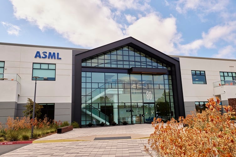
ASML has opened a new R&D facility in Silicon Valley designed to advance the company’s lithography portfolio of hardware, software and services used to generate circuit patterns on silicon in high-volume production of semiconductors.
The 212,573 square foot facility includes a Class 1000 cleanroom, lab space and collaboration areas. The facility will co-optimize IC designs, photomasks, lithography and metrology as well as inspection to enhance manufacturability and yield of leading-edge chips.
The cleanroom and lab space measures at 24,000 square feet, which the company said will be critical to enabling the next-generation of e-beam technology development and ongoing product improvements. This will include research into mechanical, optical and analog engineering as well as testing, mechatronics and more.
ASML said with the facility it is creating a new class of applications to ensure accurate wafer patterning performance and identify yield-related defects faster with greater accuracy across more wafers at the most advanced nodes.
ASML is expanding the power of computation from lithography to optical metrology and e-beam inspection as well as machine learning.
“In order to meet the next decade of scaling challenges, we need our Brion and HMI engineers to engage in an open exchange of product concepts, designs and value propositions,” said Stan Baron, general manager of Brion at ASML. “Our new campus is purposefully built with this goal in mind.”
