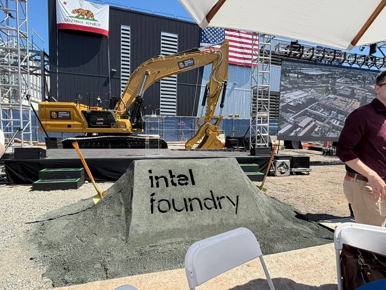
Intel Corp. has broken ground on an expansion of its Santa Clara, California, facility that will include semiconductor manufacturing capabilities for its foundry division.
The move, as reported by Wccftech, comes as Intel Foundry has garnered reportedly numerous design wins like Google, Amazon, Nvidia, Apple and maybe even rival AMD.
The expansion in Santa Clara was originally slated for middle of this year, meaning the expansion is on track. The expansion is part of Intel’s larger investment in the semiconductor ecosystem in the U.S.
This includes its two fabs it is building in Ohio and two other fabs under construction in Chandler, Arizona.
Why it matters
Intel Foundry has been looking to attract major customers for its semiconductor manufacturing business with its 14A technology and advanced packaging investments are starting to gain traction.
Earlier in 2025, it was reported that Google and Amazon were in talks with intel for foundry services for custom AI chips. These would likely be used in hyperscale data centers. Intel’s advanced packaging technology were said to be one of the main reasons for companies being interested in Intel’s foundry services.
Additionally, Intel’s 14A node has seen positive indicators from various chipmakers with electronics giants like Nvidia, Apple and AMD potential clients for the chipmaking process node. According to UBS Group, Intel may sign some formal foundry commitments later in 2026.
TeraFab
Additionally, early in April of 2026, Intel said it was joining Telsa Motors’ TeraFab project.
The TeraFab is Elon Musk’s vision for a semiconductor manufacturing gigafab that would produce chips for Tesla vehicles and robots as well as SpaceX rockets and data centers for xAI. Intel will help with refactor silicon technology in the proposed gigafab that is slated to begin production in 2029.
Packaging prowess
Part of the reason for Intel’s traction is due to its advanced packaging technologies that have become equally as important in semiconductor manufacturing as process technology.
Intel has been developing its proprietary advanced packaging since 2017 with the introduction of Embedded Multi-Die Interconnect Bridge (EMIB) and later with Foveros in 2019. At Intel Direct Connect 2025, the company said it was working on packaging offerings for its 18 A and lower process nodes with its EMIB-T iteration. EMIB-T provides denser connections, better power efficiency and lower costs, Intel said.
The EMIB-T variant would support its Foveros Direct 3D with hybrid bonding interconnects. Intel said it would allow the company to stack dies vertically on top of its state-of-the-art semiconductor manufacturing technology.
Intel already uses the packages for its own products and others. These new design wins could provide higher margins and faster revenue returns compared to full-wafer deals.
Some analysts see a future where Intel packaging becomes a main part of its core business as advanced packaging becomes more important for future hyperscale AI ecosystems.
