Extreme ultraviolet (EUV) lithography is at the center of next-generation semiconductor manufacturing as it enables smaller and more powerful microchips.
The industry is now turning to high numerical aperture (High NA) EUV systems that features NA of 0.55, compared to standard 0.33 NA. This allows for finer patterning without needing multiple patterning techniques.
High NA EUV tools will likely play a critical role in chip development in the future, particularly as processing nodes continue to become more advanced for next-generation microprocessors, memory and other electronic components.
Fine lines
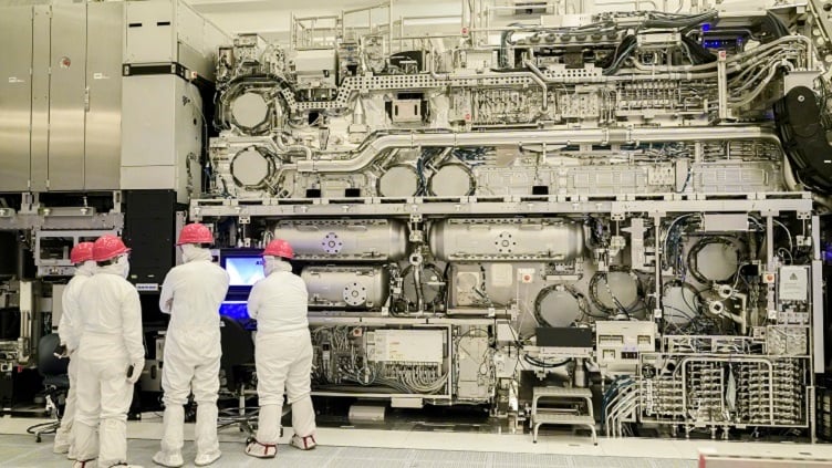
Recently, electronic test equipment giant ASML announced it printed the first 10 nm dense lines in its High NA lab in Veldhoven, the Netherlands. ASML claims these are the finest lines ever printed and set a world record for resolution on an EUV lithography scanner.
The images of the lines were printed after the tool’s optics, sensors and stages completed coarse calibration. The company said the ability to print 10 nm dense lines with a full field optical lithography system is a key step toward commercial use of the High NA EUV tool.

Early adopters
Intel Foundry, the semiconductor manufacturing division of Intel, was the first company to complete the assembly of ASML’s first commercial High NA EUV lithography scanner about a year ago in its Hillsboro, Oregon, fab. The tool will allow Intel Foundry to improve precision and scalability in chip manufacturing. It will also help to develop features and capabilities in semiconductors for artificial intelligence (AI) and other emerging technologies.
Intel also will be assembling a second High-NA EUV lithography scanner soon. In total, Intel is said to have purchased five total scanners from ASML with assembly expected over the next few years.
Intel said it will use both NA EUV lithography scanners in its most advanced process node, 18A, starting with product proof points in 2025 and then continuing into its 14A process technology into the next decade.
TSMC, the world’s largest chipmaker and foundry, is likely to assemble its first scanner in 2025. Reports said that the Taiwanese pure play foundry will use the tool for R&D initially before deploying the machines for mass production sometime in the next decade.
While only selling seven tools in the past two years may seem low, at a price point of about $350 million per tool not that many need to be sold to have an impact on ASML’s bottom line.
Market research firm TrendForce said the market is likely to see many more High-NA EUV lithography scanners installed in the coming years and likely a few this year. While so far there have been no additional sales publicly announced, orders could be anywhere between 10 to 20 machines in 2025 and beyond.
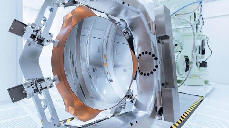 Zeiss’ precise mirror technology that is installed in the optical system of ASML’s High-NA EUV lithography scanners. Source: Zeiss
Collaborations
While ASML is currently the sole provider of High-NA EUV lithography tools, other companies are exploring how best to use the tools with the production of semiconductors.
German electronic test equipment vendor Zeiss said it has created the basic prerequisites for production of integrated circuits with an optical system inside ASML’s lithography tool. The first microchips are set to be produced in a series starting in 2025.
The optical system is an essential component of ASML’s wafer scanner as it contains mirrors that reflect light and direct it to the right spot with nanometer precision.
"Thanks to the larger numerical aperture and the new mirrors for the High-NA-EUV lithography, we can capture more light and thus expose it with even greater detail and precision,” said Peter Kürz, head of the field of business High-NA-EUV lithography at Zeiss SMT. “Experience has shown that the smaller the chip structures are to be, the larger the optical system consisting of projection optics and illumination system will be."
The illumination system for High-NA EUV lithography has about 25,000 parts and weighs six tons. The project optics weigh about 12 tons and ensure the focus of the light in the wafer scanner.
Earlier this month, Belgium research hub imec became one of the first groups to gain access to ASML’s full tool suite. The collaboration will focus on such research as sub-2 nm technology, silicon photonics, memory and advanced packaging.
This comes after the two companies opened a High-NA EUV lithography lab in Veldhoven, the Netherlands. The lab will provide logic, memory chipmakers, materials and equipment suppliers with the first prototype High-NA EUV scanner and test use cases.
Imec is preparing its extended ecosystem for the technology that includes development of:
- Advanced resist and underlayer materials
- Photomasks
- Metrology and inspection techniques
- Imaging strategies
- Optical proximity correction
- Integrated patterning and etch techniques
Conclusion
The era of High-NA EUV lithography is in its nascent stage as the first tools were sent out in 2024. In 2025, the market will likely see more orders for the machines as well as more innovations from collaborators as they get their hands on the prototype and begin to experiment with how best the technology can be used for next generation semiconductors. This should be a year-long trend that will only pickup in subsequent years.
