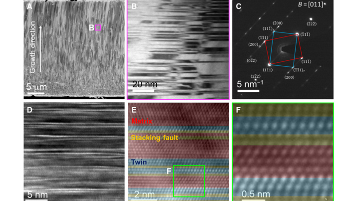
 Cross-sectional microstructure of the alloy film as deposited. (Credit: Johns Hopkins)Silicon can only do so much.
If you do any reading on technology’s future – and my guess is that if you’re here, you do – it’s a theme you’ve probably heard repeated many times. Silicon has, of course, been at the heart of microelectromechanical systems (MEMS) fabrication for many generations; most MEMS devices have internal silicon structures smaller than the width of a human hair. But silicon is brittle and prone to break. Add a modest amount of heat, and the silicon devices can lose their strength and their ability to conduct electronic signals.
These are just the sort of conditions that will limit silicon’s future as we move into development of the Internet of Things (IoT), the interconnected network of MEMS devices in which everything from appliances to jet engines to oil rigs can be remotely monitored and controlled.
Enter Kevin J. Hemker, a materials scientist and mechanical engineer at Johns Hopkins University. As reported in the current issue of the journal Science Advances, Hemker and his team are pursuing the development of new materials with greater strength, density, and electrical and thermal conductivity that withstand high heat and physical stress. The materials can also be made and shaped at the microscopic scale.
Supported by a National Science Foundation grant, the researchers explored combinations of metal containing nickel – a common ingredient in advanced structural materials. Jet engines, for instance, employ nickel-based superalloys. Pure nickel expands in heat, but adding molybdenum and tungsten curbs that tendency, providing greater dimensional stability.
The team’s research has led to the creation of freestanding alloy films. In the lab, the team hit targets with ions to vaporize alloys into atoms and deposit them onto a substrate. This created peel-away films with extraordinary properties – such as a tensile strength three times greater than high-strength steel. With an average thickness of just 29 microns, less than the thickness of a human hair, the films can withstand high temperatures and are both thermally and mechanically stable.
Hemker says that atomic-scale patterning of the alloy’s internal crystal structure – a combination of solid solution strengthening and the presence of dense nanotwins – is responsible for giving the material strength without impeding its electrical conductivity. The structure "has given our films a terrific combination, [a] balance of properties," he said. The team has filed a provisional patent application for the alloy.
The next phase of development is to shape the films into MEMS components. Stay tuned.
