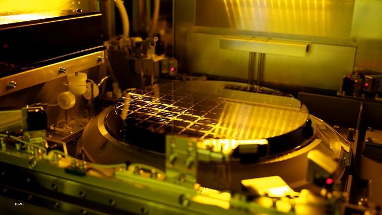
Nvidia and the world’s largest foundry TSMC are collaborating to speed up semiconductor design and manufacturing.
Under the deal, TSMC will use Nvidia’s AI and computing chips across its semiconductor design and manufacturing lifecycle to improve turnaround time, energy efficiency, yield and operational productivity in fabs.
“NVIDIA and TSMC have worked together for nearly three decades to push the limits of computing,” said Jensen Huang, founder and CEO of NVIDIA. “TSMC is bringing NVIDIA AI and accelerated computing into the fab itself, tackling some of the world’s most complex design and manufacturing challenges with simulation, optimization and AI to improve speed, efficiency and yield for the next generation of chips.”
The companies said the AI and computing chips will provide support for:
- Computational lithography
- Transistor simulation
- Process control
- Wafer inspection
In terms of computational lithography, TSMC is using Nvidia cuLitho, a GPU-accelerated library for lithography, which delivers 20% to 50% improvement in cost effectiveness or cycle time compared to CPU-based computational lithography.
In transistor simulation, TSMC is using Nvidia cuEST, a CPU-accelerated electronic structure simulation library for 50 times faster chemistry simulations, Nvidia said.
TSMC is using Nvidia CuML machine learning library for advanced process control for large-scale analytics on Nvidia GPUs. This will allow the foundry to speed algorithms and generate hundreds of thousands of process parameters spanning thousands of steps for precision inputs for machine learning models.
Finally, TSMC is using CUDA-power computation on Nvidia H200 GPUs to enhance its capability to manage complex constraints and streamlines production paths and fab productivity.
Defect detection
Additionally, TSMC is using Nvidia Metropolis with Nvidia Tao toolkit for defect classification that will utilize vision AI to find chip defects at nanometer scale. The companies said this will improve inspection while reducing repeated labeling and process conditions.
TSMC is also exploring Nvidia Omniverse libraries to build a FabTwin, or a virtual fab environment for evaluating process tools and simulation workflows. This will help the foundry to compare configurations with more flexibility and identify constraints earlier.
