
On the wide-bandgap semiconductor landscape, the outlook for gallium nitride (GaN) foundry services seemed set to crack and split following recent events.
Concerns rose when major foundries departed, led by TSMC's announcement of its GaN exit; however, with ample warning, most customers quickly found alternatives.
Wolfspeed also pulled back after a brief bankruptcy and rapid restructuring, refocusing its foundry business on pure-play silicon carbide (SiC). Integrated device manufacturer (IDM) NXP Semiconductors is also exiting GaN after a perhaps ill-timed 2020 investment in its 150 nm GaN fab.
With some big names out, a few insiders wondered if a wave of lower-priced Chinese GaN foundries could disrupt the market entirely. Others, notably Innoscience’s founder and chair Luo Weiwei, worry about the GaN foundry model altogether, suggesting that simpler consumer power devices might fall to IDMs, leaving only more complex GaN chips for foundries.
Yet, out of brief chaos may come orders. More foundries are entering the market, and some are teaming up to pursue global opportunities, while analysts remain bullish on GaN overall. Grand View Research estimates the market at $12.47 billion by 2030, up from $3 billion at the close of 2024. Spherical Insights projects similar annualized growth further out, to $ 38.83 billion by 2035.
One analyst cites a combination of factors in play. “Pricing pressure is likely to persist over the next one to three years but should not be viewed as a long-term structural issue,” said Rany Gong, analyst at TrendForce. “Ultimately, competitive positioning will be determined by scale, yield, reliability, and system-level solution capability — rather than pricing alone." Scale may be a ways off yet, as 300 mm GaN tools are still scarce; however, with imec building a 300 mm ecosystem and other developments, tools should close the gap soon.
Undaunted by the challenges, GaN foundries seem to be converging on three system-level solutions, with two of them on a collision course with GaN IDMs after the same solutions. Examining these solution categories in greater depth sheds light on the strategies at play.
mmWave and sub-THz RF devices
GaN offers advantages for high-performance, high-power RF power amplifiers, filters, mixers and switches at millimeter-wave (mmWave) or sub-THz frequencies. These devices place a premium on performance and reliability, are far less sensitive to price competition, and often use unique foundry processes, making alternative sourcing difficult and creating at least a partial barrier to IDM entry. GaN-on-SiC offers higher power capability, while GaN-on-Si scales to 200-mm and 300-mm wafers, improving CMOS process integration and ultimately driving down costs.
Radar, electronic warfare and secure communication systems are essential to today’s warfighters, and there are many low- to mid-volume opportunities for highly customized RF devices with extended environmental specifications.
Serving defense customers is a cluster of accredited U.S.-based GaN foundries screened by the Department of Defense (DoD) under the Trusted Foundry Program.
Entering 2026, six locations hold GaN foundry accreditation. This includes:
- BAE Systems Microwave Electronics Center in Nashua, New Hampshire
- MACOM in Lowell, Massachusetts
- Northrup Grumman Aerospace Systems in Redondo Beach, California
- Mission Systems in Linthicum, Maryland
- Raytheon RF Components in Andover, Massachusetts
- Qorvo in Richardson, Texas
A recent development is a partnership between HRL Laboratories and MACOM on HRL’s 40 nm T3L GaN-on-SiC process, a three times shrink beyond processes offered by most trusted foundries. HRL innovated T3L from the US Navy’s SOTA Radio Frequency Gallium Nitride (STARRY NITE) program, and MACOM is bringing it into their trusted foundry for high-volume production.
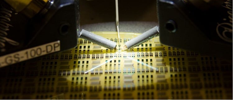 HRL Laboratories, a GaN foundry, is working with the Department of Defense for GaN technology in broadband RF applications. Source: HRL Laboratories
High-performance RF devices also power 5G and 6G communications infrastructure, including terrestrial base stations, Low Earth Orbit (LEO) satellites in non-terrestrial networks (NTNs) and automotive platforms.
GaN foundries are jockeying for position in GaN for 5G/6G devices including:
- Agnit Semiconductors
- Finwave Semiconductor
- HRL Laboratories
- MACOM
- Qorvo
- RFHIC
- Sanan IC
- Sumitomo Electric
- United Monolithic Semiconductors (UMS)
- WIN Semiconductors
- X-FAB
High-voltage DC distribution architectures
Pushing higher-voltage GaN transistors into what used to be exclusively SiC territory positions GaN for a new vision of DC power distribution. Chips targeting AI training are consuming massive amounts of power, 1,000 W or more for each chip, exposing the inefficiency of AC-to-DC conversion within every subrack.
Projections of up to 1 MW per rack in an “AI factory” make efficiency imperative. Momentum is building around an NVIDIA-backed concept for high-voltage DC (HVDC) power distribution in AI data centers, centered on 800 V DC, which eliminates conversion losses at multiple points and eases energy storage integration.
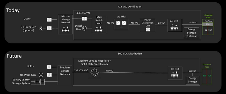 Nvidia is moving from 415 V AC (top) to 800 V DC power distribution (bottom) using GaN power semiconductors. Source: Nvidia
Electric vehicles (EVs), where weight and efficiency translate to range, route enormous amounts of DC power among their charging, storage and propulsion subsystems. EVs are also moving from the prevailing 400 V DC architecture used by most manufacturers to an 800 V DC architecture providing faster charging, more efficient power distribution, reduced weight and size (for example, by using smaller-gauge, lighter wiring that carries less current), and lower thermal dissipation. Systems combining photovoltaic panels, power distribution units and battery storage, such as solar energy generation and satellite power systems, also hinge on efficient DC power distribution and will likely follow a similar profile.
Most GaN HEMTs today are in the 600 V DC to 700 V DC range, combining fast switching with high-power handling to improve efficiency, reduce package size and manage thermal dissipation. For 800 V DC conversion, teams are innovating switched-mode architectures, such as Navitas Semiconductors’ proposed three-level half-bridge, using 650 V GaN transistors on the primary side and 100 V GaN transistors on the secondary side.
However, GaN's voltage limitations may soon change. Research teams at GaNPower International recently demonstrated 1,200 V EMODE GaN FETs, raising the bar further into territory previously exclusively occupied by SiC power devices.
Device power for consumer electronics
Device power, whether it comes via an external brick or is embedded in an outlet-pluggable or standalone device, sometimes in a big device like a car, is a ubiquitous feature in consumer electronics. Unlike the two segments discussed earlier, pricing pressure on chargers and power supplies is intense, as they are often bundled with consumer devices, heightening the urgency for 200 mm and 300 mm GaN wafers. High power density in small packages is also a priority.
Supplying power-conversion parts is an area where Asian GaN foundries are making headway. PSMC is replacing TSMC as Navitas' primary GaN foundry, thanks to a similar process technology easing the transition. Vanguard International Semiconductor (VIS) has also secured a TSMC process license for consumer power applications. After lining up customers and capacity, Samsung Electronics' long-rumored entry into GaN power chip foundry appears imminent.
A couple of other Korean firms, DB HiTek and SK Keyfoundry, are also preparing their GaN foundry offerings. In Europe, X-FAB is plowing ahead with 200 mm GaN-on-Si wafers for consumer power. Teaming arrangements among GaN foundries/IDMs across different continents are taking shape, with onsemi partnering with GlobalFoundries (another TSMC licensee) and Innoscience. More IDMs in the mix for consumer and automotive GaN parts include Infineon, Rohm Semiconductor, ST Microelectronics and Texas Instruments.
Conclusion
Pessimism about the GaN foundry model seems premature, but strategies may shift as these system-level solution needs become clearer. Foundries have an advantage in highly customized RF devices, especially for defense use. IDMs may have an edge in power conversion with off-the-shelf catalogs of GaN switching devices, though there is still room for innovation from fabless GaN firms in HVDC power distribution. Both sides will drive for larger wafers and lower costs, likely chipping away at SiC market share as GaN power capabilities improve.
