In July, the world’s largest chipmaker and foundry Taiwan Semiconductor Manufacturing Co. (TSMC) said it would exit the gallium nitride (GaN) semiconductor segment, citing that the low-margin, low-volume business was not in its strategic future.
Add to this mounting price pressure from Chinese rivals, TSMC plans to phase out its GaN foundry services by July 2027, focusing squarely on leading edge semiconductor manufacturing.
TSMC makes its money on cutting edge semiconductors in smartphones, data centers, media tablets and servers. While the foundry’s prices may be higher, according to a recent statement from microprocessor giant AMD, it is worth it.
But for TSMC, GaN is not.
“It doesn’t make sense for TSMC to focus on older process nodes or specialized technologies like GaN,” said Phil Solis, research director of client processors and connectivity at market research firm International Data Corp. (IDC). “There are good applications for GaN, but they are not at the volumes or the revenue that TSMC would get from applications like smartphones and data centers.”
However, for other vendors it is worth it. Particularly those already in the mobile network or RF device segment.
Who stands to benefit
TSMC exiting the GaN market is only a boon for those vendors already equipped to build the semiconductors and those gearing up for expansion.
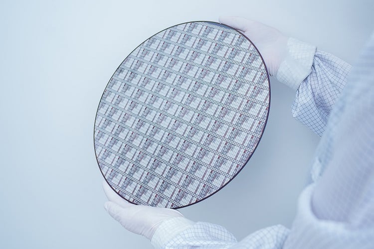
Shortly after the news that TSMC was planning to end its wafer foundry services for GaN by 2027, Infineon Technologies — a maker of silicon, silicon carbide (SiC) and gallium nitride chips — said it will ramp up its efforts to scale up its GaN production on 300 mm wafers. It plans to have the first customer samples of these devices before the end of 2025.
Infineon said its GaN semiconductors will be designed for smartphone chargers, industrial robots, solar inverters and more. The 300 mm wafers are superior and more efficient than 200 mm GaN wafers with a larger size yield of 2.3 times more chips per wafer, Infineon said.
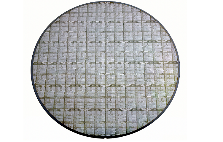
 Infineon engineers show its 300 mm GaN power wafer. The company has developed a wafer grinding approach that influences handling and processing of the backside of the wafer. Source: Infineon
Solis said he expects to see similar ramp ups of GaN technologies from those players already in the market such as:
- Texas Instruments
- NXP Semiconductors
- GlobalFoundries
- United Microelectronics Corp. (UMC)
- Powerchip Semiconductors Manufacturing Co. (PSMC)
“Depending on the application, GlobalFoundries will pick up some of the business from TSMC, and these other companies will pick up some of the other business that TSMC will no longer have,” Solis said.
Other deals are already happening. Also in July, Incize and Atomera signed a collaborative agreement to enhance GaN-on-Si technologies to accelerate volume production for next-generation RF and power devices.
The deal will focus on optimizing GaN-on-Si for high-frequency and high-power applications like:
- 5G/6G wireless infrastructure
- Satellite communications (SATCOM)
- Power electronics
Fallout of TSMC’s exit
After TSMC’s announcement, Navitas Semiconductor shifted its production to smaller Taiwanese foundry PSMC to ensure it receives a continued supply.
According to reports, TSMC’s current 6-inch monthly output for GaN is about 3,000 to 4,000 wafers. Of this, Navitas and Ancora Semiconductor accounted for more than half of TSMC’s GaN volume.
Navitas’ choice of PSMC comes down to technical compatibility, according to Anue. Both use GaN-on-Si technology, so it should be a natural transition for the vendor.
Chinese players
Much like other wide bandgap technologies, Chinese vendors are actively ramping up production of GaN chips such as Chinese vendor Innoscience, which claims it is operating the largest dedicated 200 mm wafer GaN-on-Si manufacturing capacity globally.
More GaN-focused Chinese vendors are likely to ramp up production of these devices due to their ability to offer cheap prices compared to others in the market. This will come despite grow margins being a key challenge for these domestic Chinese vendors.
Some have speculated that price pressure is one of the main reasons for TSMC’s exit from the GaN sector. Since the foundry already has limited scale and GaN is not a major moneymaker, it was easier for TSMC to just exit the sector rather than engage in the hassle of a price war.
However, aggressive pricing from China will be a major challenge for those vendors remaining in the GaN market in the future.
Why GaN?
Specialized processes like GaN cost more, but they are needed in certain applications.
Some technologies can be accomplished in CMOS and most companies wish for this because it is the cheapest technology. According to IDC’s Solis there were technologies like RF that were not possible to do previously in CMOS, but they figured out how to do it for applications like Bluetooth and low-power Wi-Fi.
But for larger RF applications, such as base stations or robotics, CMOS won’t work, and technology like GaN is needed due to its features like:
- High efficiency at high frequencies
- Delivery of high-power density
- Better thermal performance
- Longer device lifetime
- Smaller form factor
