
Ever since the first Ajinomoto Build-up Film (ABF) shipped in 1999, ABF has remained the dominant material used for fine-pitch routing layers in integrated circuit (IC) packaging. Onshoring transitions are driving new semiconductor production capacity, with major facilities coming online in the U.S. and more broadly in Southeast Asia outside of China. However, packaging capacity has lagged, and semiconductor manufacturers still need to ship their advanced chips overseas to be packaged.
An important part of that supply chain is access to materials and fabrication capacity in the U.S. Newer materials, which were previously in the research phase, are now finally being commercialized. Going forward, applying these materials in packaging can be achieved through a combination of materials availability and advanced processing for building IC substrates.
Still, there’s a question as to whether this area can attract sufficient public or private investment to build the capacity needed to package enough chips for the U.S. market. Has the ball finally started rolling in the right direction? We will examine the current state of packaging, materials and capabilities in this article.
The packaging issue is becoming mainstream
Ever since the CHIPS Act was first proposed in 2020 and signed into law in 2022, much of the discussion regarding electronics in the mainstream media has focused on semiconductor fabrication. Packaging people know that their technologies tend to take a backseat to semiconductors, and the AI revolution has only exacerbated that problem. Advocacy for greater packaging capacity and capability has since been championed by several industry groups, including the Global Electronics Association, Printed Circuit Board Association of America and United States Partnership for Assured Electronics.
A recent New York Times article drew attention to the packaging issue and finally recast it in the context of the supply chain for the chips used for AI compute. The important takeaways include:
- U.S. market share of advanced packaging capacity sits at only 3%.
- Meanwhile, TSMC handles 95% of advanced packaging and is 30% short of fulfilling demand.
- That means chips fabricated in the U.S. must still travel to Taiwan to be packaged.
For those viewing this in the vein of national and economic security, this represents a serious vulnerability, particularly if a future conflict with China were to manifest itself.
“The semiconductor conversation in the U.S. has focused heavily on fabrication,” said John W. Mitchell, president of the Global Electronics Association (formerly IPC), who noted the issue in a post on social media. “Packaging has been treated as an afterthought for decades, offshored to lower-cost countries with little thought to what that dependency would look like under pressure. Now we are seeing what it looks like.”
Now, investment capacity is coming to the U.S. from some of the biggest names in semiconductor manufacturing — a capability that should be obvious to any outside observer. And while there is capacity investment, there is something else below the surface that is a major determinant of electrical performance and manufacturability: substrate materials.
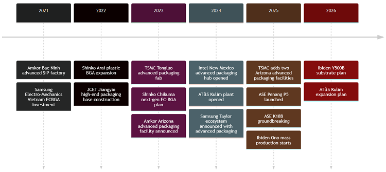 Semiconductor company investments in packaging/substrate capacity since 2021 (current as of July 2026).
Substrate materials make it possible
IC substrates are part of the electrical architecture that determines how much bandwidth, power and routing density can be brought into a monolithic or multi-die system. Large AI accelerators, high-bandwidth memory (HBM) stacks, chiplet assemblies and interposers all require fine lines and spaces, low dielectric loss and dispersion, and enough mechanical reliability to survive assembly and field operation.
Conventional ABF materials made this class of packaging possible, but the next generation of AI packages is pushing substrate materials closer to their limits. But from a supply chain perspective, this is quite dangerous, as ABF enjoys a near monopoly in the built-up film market. The technical demands of advanced chips, particularly for AI compute, as well as the supply chain risks inherent in ABF, are helping drive innovation in new substrate materials and manufacturing processes.
Some of the newest substrate material sets being commercialized for package fabrication include:
- Advanced homogeneous isotropic thermoset resins (Thintronics)
- Thin liquid crystal polymer (LCP)/bonding layer pairs (Precision Circuit Technologies)
- Zero and negative coefficient-of-thermal-expansion (CTE) films and negative-CTE films (Advanced Chip and Circuit Materials)
- Ultra-thin copper-coated resins (AGC Multi Materials)
These materials are typically laminated on a rigid core (e.g., BT epoxy or similar) in packages that implement organic substrates. They generally have dielectric constants (Dk) of approximately 3 or lower, as well as low loss tangent (less than 0.005) and low skew/no skew compared to glass-reinforced epoxy resin materials.
Each of these options overcomes certain technical challenges related to signal integrity (SI), manufacturability and multi-die integration. But to overcome supply chain challenges, there needs to be a corresponding fabrication process tailored to the materials in question.
Now, only Precision Circuit Technologies has tailored a proprietary semi-additive process (SAP) for use with LCP materials, giving linewidths and trace spaces as small as 6 microns. Access to this level of density in volume production is what's needed to rebuild packaging capability and capacity in the U.S.
“Our process controls for very small linewidth and tighter tolerances than existing semi-additive approaches,” said Jim Rathburth, CEO of Precision Circuit Technologies. “The highest density packages demand this level of precision and it’s difficult to find at scale, but it’s where the industry needs to go in order to build packaging capacity for high-demand areas like AI processors.”
Where investment dollars will go next
The materials listed above do not strictly require a proprietary deposition process to form copper features on the build-up film layers or core layers in the substrate stackup. The SAP and modified semi-additive process (mSAP) approaches used in IC substrates can be adapted to these material sets, so with sufficient investment, it is conceivable that the major semiconductor manufacturers, outsourced semiconductor assembly and test (OSAT) providers and equipment/process suppliers can build capacity quickly.
Real investment in packaging capacity needs to follow the electrical and manufacturing constraints that now limit AI processors at the package level. New substrate materials can reduce loss, improve dimensional stability and support finer routing, but those gains only matter when they are paired with repeatable SAP or mSAP processing, qualified lamination flows and reliable via formation. Domestic capacity will remain incomplete until substrate fabrication can support the density, yield and process control required by the silicon it is meant to package.
