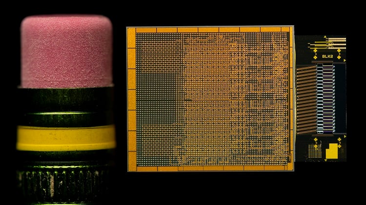
Most people know me as a PCB guy, but in my adventures in electronics design I have found that many of the reliability problems in PCBs have their doppelgangers in packaging. Chiplets are poised to usher in the next great shift in component design, yet design of chiplet-based components brings a set of design and reliability challenges that have their similarities in high-density PCB/package substrate design with monolithic dies and conventional high-density components.
Chiplet designs are important as they are one way to keep advancing density and performance despite the slowdown of Moore’s Law. From a product development perspective, chiplets promise a faster time-to-market by leveraging off-the-shelf dies and shifting the design effort into packaging and interconnect design, rather than focusing on die design directly. Along with this main benefit comes significant challenges in reliability, testing and verification that must be addressed for chiplets to fulfill their promise.
Reliability challenges in chiplet-based designs
Building a multi-die system introduces reliability concerns beyond those found in traditional SoC designs. From a product reliability standpoint, chiplet designs must meet the stringent quality standards of their target markets. This is pushing chiplet integrators to perform extensive qualification testing on assembled packages, subjecting devices to heating/cooling cycles, thermal shock, vibration and other tests to determine true defect levels in multi-die assemblies. Some of these reliability tests and challenges have their analogues in packaging for monolithic dies and in ultra-high-density PCBs.
The black box problem
A major verification hurdle in chiplet-based designs is the black box problem. Third-party chiplets could be IP bought from a marketplace, or they could be provided from an external vendor’s die, and the designers or test engineering might not have full visibility into its internals. Standard interfaces like UCIe are helpful as this eliminates guesswork on I/O or chiplet-to-chiplet interfaces because compliance and stress tests are standardized. But custom interfaces and power subsystems will not be standardized and there will have to be a reliance on vendor models for verification and simulation.
Unfortunately, vendor models of custom interfaces and power subsystems are not always correct reflections of reality. This is an open area in the industry that exists due to a lack of standardized testing and data communication formats between vendors. This has driven the preference for using proven silicon in new chiplet-based designs, where vendor chiplets reuse dies that have already demonstrated reliability and functionality in other designs.
Coplanarity
The structure of chiplet-based designs involves bonding microbumps to pads on a substrate in order to make electrical connections. In these structures, mechanical stress accumulation during assembly and during operation of the component creates a reliability challenge. The package needs to maintain coplanarity with the chiplets on the package substrate to prevent a component failure during assembly or during operation.
- During assembly — Excessive deformation at the bump-substrate interface could result in a weak connection or open connection
- During operation — Uneven deformation within the package leads to stress accumulation or fatigue from thermal cycling, creating a point of failure
Ensuring co-planarity of dies during assembly is exceedingly difficult with planarity requiring control to 1 in 100,000 bumps. Any slight bowing at the substrate/bump interface can lead to poor connections after solder reflow. Advanced packaging houses are now investing in higher-precision metrology tools to measure and correct coplanarity during assembly. Newer organic materials for package substrates, as well as underfill, adhesives and low-temperature solders, are being developed to have closer matching of CTE values to provide stress mitigation.
Testing complexities in multi-die chiplet systems
Testing in chiplet-based systems is far more complex than in monolithic SoCs. Each die (chiplet) must be tested individually and again after integration, requiring multiple test stages. A key concept is the Known Good Die (KGD), meaning chiplets must be verified before assembly to avoid costly scrap of multi-die packages. This demands built-in test structures and high-coverage wafer-level testing.
Testing occurs at several stages:
- Pre-bond testing (KGD): Verifies individual chiplets' logic and memory via probe pads or test interfaces.
- Mid-stack testing: Assesses die-to-die and die-to-substrate interconnects after bonding, catching defects like shorts or misalignments.
- Post-assembly testing: Exercises the full package and chiplet interactions.
- System-level testing: Involves board-level stress tests (thermal, software) to uncover issues missed in lab tests.
Challenges include probing fine-pitch micro-bumps and maintaining test access throughout 3D stacks. Solutions include built-in self-test (BIST), sideband test signals (e.g., in UCIe) and standards like IEEE 1838, which defines “test elevators” to access buried dies.
Interconnect testing is particularly demanding, with thousands of connections requiring efficient test patterns. For example, Imec’s E²I-TEST improves coverage by detecting subtle resistive defects with a small, scalable pattern set. Standardization is advancing, with IEEE P3405 working on unified procedures for interconnect testing and in-field repair. These efforts aim to enable interoperable, high-yield chiplet systems across vendors.
Where chiplet designs go from here
My view has been that chiplets will become commoditized, and many of the reliability and testing challenges surrounding chiplet-based designs will ease as a marketplace for these products matures. When you think about it, the chiplet market is not fundamentally different from the IP core market or the electronic component market, and standardization has developed within those market segments to aid manufacturing, testing and verification.
As more standardization develops in these areas, and as materials and test methodologies improve, chiplets should democratize chip designs for smaller companies and even individual entrepreneurs.
