Semiconductor testing has traditionally functioned as a stable screening step in the manufacturing flow so that failing devices can be identified and separated prior to packaging. Test infrastructure was not originally designed to accommodate the challenges of advanced process nodes, multi-die assemblies, and high-frequency switching operations during test. More advanced chips are putting more requirements on test probes due to the complex physics arising while testing these more advanced semiconductor products.
We find three major challenges are currently inhibiting the accuracy of test probe implementation:
- Coupled physical interactions at the probe tip
- Inconsistent requirements in multi-die/chiplet assemblies
- Switching speeds in probe test equipment
The high-level result of failing to address these challenges is inaccuracy in terms of throughput and yield, where false failures are identified, true failures are missed and the overall testing process takes longer.
Mechanical stress creates coupled physical interactions
Wafer probes were historically optimized around predictable pad geometries, moderate I/O counts, and relatively forgiving mechanical tolerances. As pad pitches shrink and I/O counts increase, the act of making contact becomes increasingly sensitive to planarity, alignment and force control. Probe cards must simultaneously maintain electrical continuity and avoid damaging the device structures during probing.
Modern wafer probes are mechanically aggressive, particularly for large die and dense layouts. Uniform force distribution across the probe array is difficult to maintain, and even small deviations can result in localized stress. Higher density dies are more likely to experience probe-induced mechanical signatures, which decrease the long-term reliability.
The primary mechanical stress factors in modern wafer probe implementations include:
- Shrinking pad pitches and increased I/O density
- Reduced margin for probe alignment and overdrive
- Uneven force distribution across large/non-uniform dies
- Accelerated probe wear
- Debris accumulation at contact points
- Contact resistance becomes more sensitive to mechanical variation
The test challenges present in advanced packages, multi-die assemblies and chiplet-based designs have been known for some time but have become increasingly prevalent as more companies reach advanced nodes or multi-die/chiplet capability.
“It's very, very difficult to do dynamic testing on chips and some of the advanced packaging formats,” said Phil Marcoux, industry veteran and charter member of SMT Council at IPC. “Even flip chips, for example, are problematic because if you probe them you potentially damage the balls and you find it difficult to get accurate dynamic or AC testing in some cases."
From a process standpoint, wafer probe operation is becoming more metrology-aware, where contact resistance trends, probe mark inspection and force optimization are used together to reduce mechanical damage while maintaining electrical continuity. These approaches reflect a broader recognition that probe performance must be actively managed as a mechanical system, not just an electrical interface.
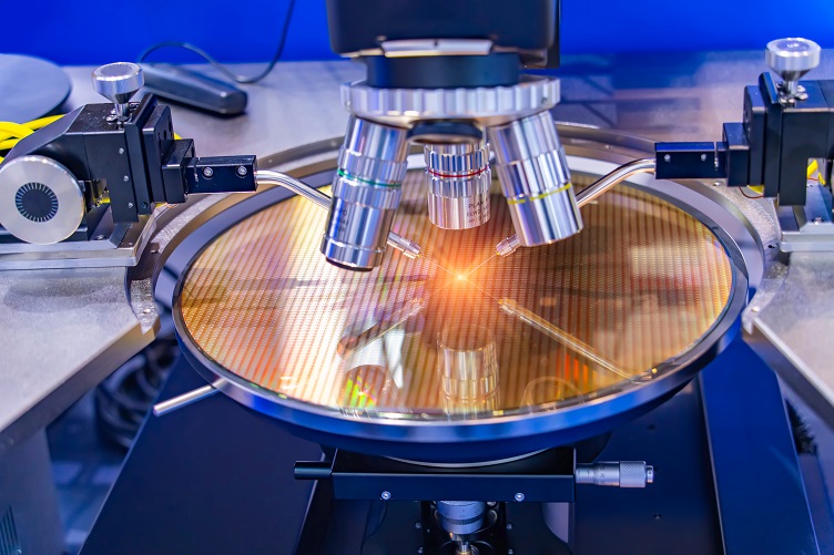
 A photo of a wafer probe. This type of testing is a screening step in the manufacturing flow to identify failing devices. Source: S!mon/Adobe Stock
Multi-die assemblies must redefine “known good die”
The transition toward heterogeneous integration and advanced packaging further complicates the use of a wafer probe. For example, chiplet-based assemblies, 2.5D assemblies and 3D assemblies contain uneven surfaces, inconsistent height, varying material stacks and complex mechanical responses to the probe tip create complex coupling of electrical, mechanical and thermal behavior during probe contact.
Due to the multiple physical responses at play during probe contact, electrical pass-fail results alone are no longer sufficient to define device quality. Mechanical damage may not immediately manifest as a failure but can reduce yield during assembly or compromise long-term reliability. As a result, probe strategy directly influences manufacturing economics, particularly for high-value wafers at advanced nodes.
The table below summarizes how traditional probe assumptions differ from those required for modern multi-die devices.
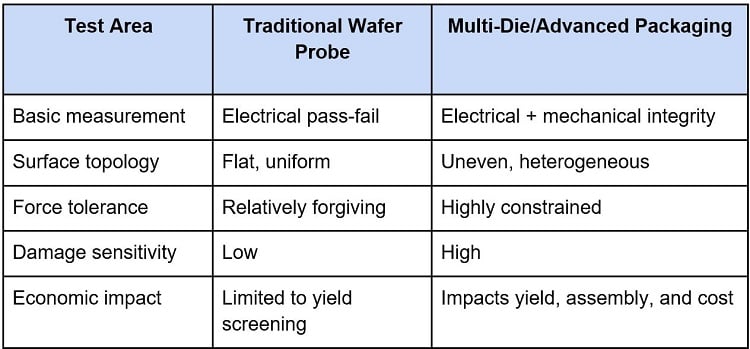
To address these challenges, some test flows are evolving to treat wafer probe as a risk-reduction step rather than a final QC step. These changes reflect the reality that heterogeneous assemblies have mechanical integrity requirements during probe operation, which are just as important as electrical defects detection.
Signal switching limits in multi-GHz SoC test
While wafer probe challenges are largely mechanical, SoC test systems face another electrical challenge. Modern SoCs operate across multi-GHz RF, multi-Gbps digital and precision analog domains. This demands a clearer focus on signal integrity within the tester itself during test signal generation. In these environments, the signal switching action is a primary determinant of measurement accuracy and repeatability.
Electrical performance requirements driving switching challenges include:
- Low and stable probe contact resistance
- Low capacitance and leakage for high-frequency signals
- High insulation resistance for precision analog measurements
- Repeatable performance over billions of switching cycles
High-frequency switching action occurs in large switch matrices, where the physical structure introduces parasitic capacitance, resistance and leakage that directly affect high-frequency measurements. The parasitic capacitance acts as a source of crosstalk that leads to false errors, while resistance and leakage act as sources of signal loss, which reduce available margin in the test setup.
Switch matrices also need to be stable at high frequencies, referring to stable output frequency, amplitude and transients. At higher operating frequencies, small variations in switching behavior can create greater inaccuracies in test results, which may lead to false failures and thus artificially reduced yield. Switching performance therefore defines the practical limits of test capability independent of instrumentation resolution.
Phil Marcoux noted how dynamic testing and burn-in must change to accommodate more advanced multi-die/chiplet-based assemblies. This creates challenges for new companies developing chiplet-based products.
“Dynamic testing may come burned in, and there's things that a packaged part gets that a chiplet will not get, therefore the designer is going to be faced with compromises,” Marcoux said. “That has been a severely limiting factor…that creates barriers to entry for companies who want to get into this space.”
Within test equipment design, an important determinant of stability is the primary switching stage component. RF reed relays are one component used in this context due to their stable electrical switching characteristics at the relevant frequencies used in precision test platforms for advanced nodes. These components have hermetically sealed packaging and have more stable switch action that helps ensure consistent contact behavior over long operational lifetimes.
Semiconductor test is no longer a fixed infrastructure element that can be scaled independently of device design. Mechanical probe behavior, packaging design and signal switching are now factors that influence yield, reliability and product cost. As devices continue to scale in complexity and operating frequency, test increasingly operates at the boundary between manufacturability and theoretical performance, rather than being a simple validation step.
