Lam Research has introduced a deposition tool designed for next-generation semiconductors to solve manufacturing challenges like 3D stacking and high-density heterogeneous integration.
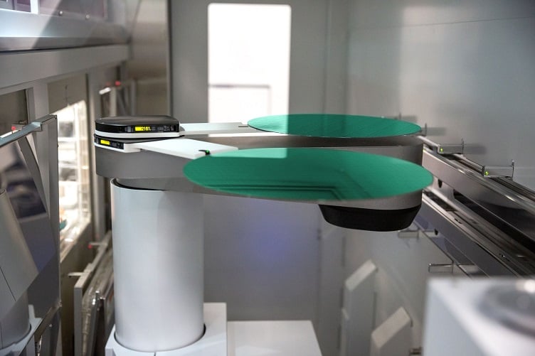
Called the Vector TEOS 3D, Lam said the tool will be required for applications like AI and high-performance computing (HPC) applications. The tool provides ultra-thick, uniform and inter-die gapfill using a bowed wafer handling approach as well as dielectric deposition and monitoring through Lam Equipment Intelligent technology.
"VECTOR TEOS 3D deposits the industry's thickest, void-free, inter-die gapfill films, customized to meet the challenging requirements of advanced die stacking integration schemes, even on ultra-stressed, high-bow wafers," said Sesha Varadarajan, senior VP of the Global Products Group at Lam Research. "It's another powerful addition to our best-in-class advanced packaging portfolio, which delivers the differentiated, atomic-level innovations chipmakers need to scale beyond Moore's Law and into the AI era."
Other features include:
- Single-pass processing of crack-free film more than 30 microns thick
- Quad station module architecture
- Lam Equipment Intelligence technology for process repeatability
- Integrated RF generators and ECO mode peripherals control
Why is it needed
Lam Research said the growth of AI is leading to new devices having to support data-intensive workloads. Because of this, chipmakers are using 3D advanced packaging to integrate multiple dies into chiplet architectures to enable AI computing prowess.
Chiplet designs can improve processing speed and are able to pack more memory and processing closer together in electrical pathways for more power. But as these chiplets scale taller and become more complex, new challenges emerge from the stress during processing that can distort or bow a wafer’s shape.
The TEOS 3D tool has nanoscale precision and can deposit specialized dielectric films of up to 60 microns thick between dies with scalability to deposit films greater than 100 microns. This provides structural, thermal and mechanical support to prevent common packaging failures such as delamination, Lam Research said.
Additionally, the tool has clamping technology and pedestal design that provides stability when processing thick wafers.
