Chip manufacturing equipment supplier ASML Holding NV has received an order for 15 extreme ultraviolet (EUV) lithography systems from an unnamed U.S. customer. The order could be worth in excess of $1 billion.
The customer is almost certainly Intel, one of few global chip manufacturers contemplating the use of EUV lithography for possible insertion at the 10nm or 7nm manufacturing process nodes.
While ASML did not name the customer, Len Jelinek, senior director of semiconductor manufacturing at IHS Technology, says, the tools are for Intel. "Intel is preparing for 10nm manufacturing and the use of EUV will allow them to get back on the cost-reduction part of Moore's Law," Jelinek says.
 Current expectation for EUVL production insertion. Source: ASML.
Intel (Santa Clara, Calif.) did not immediately respond to request for comment on the EUV tool order.
The EUV systems will be used to support increased development activity and pilot production of chips, with delivery of the first two NXE:3350B systems expected before the end of 2015, says ASML (Veldhoven, the Netherlands) in a statement. The tool supplier adds that the new tools will be in addition to existing EUV development systems already with the customer—another clue that points to Intel, one of three chip vendors that has invested in ASML to help fund EUV development.
Deliveries of the orders are likely to be spread into 2016 and even into 2017, but they represent a significant vote of confidence in a technology that has been under research since the mid-1980s and under development since the late 1990s.
 Len Jelinek
Jelinek says Intel engineers have been able to do additional engineering to improve EUV lithography productivity. "Intel has been able to modify the tools in order to optimize performance and achieve throughput in excess of 100 wafers per hour. This clearly offers cost advantages over double- or triple-pattern processes," Jelinek says.
While source power has been the No. 1 concern facing EUV lithography due to its impact on productivity, progress is also needed in mask infrastructure, resists, pellicles and inspection.
But technical progress with EUV has started to get on a roll in recent months. Late in 2014, foundry Taiwan Semiconductor Manufacturing Co. Ltd. (Hsinchu, Taiwan) ordered two NXE:3350B EUV lithography systems for production use that are expected to be delivered in 2015.
In February, ASML and TSMC announced that TSMC had exposed 1,000 wafers on an NXE:3350B system in one day. This level of productivity was a marked improvement from the previous high of 500 wafer exposures per day in endurance tests just three months earlier.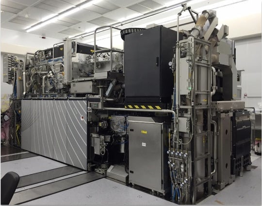 3350B EUV lithography system being prepared for shipping in mid-2015 with high-power laser and in-situ collector cleaning. Source: ASML.
During a conference call with financial analysts held on April 15, ASML CEO Peter Wennink, said the overall target for 2015 was production of 1,000 wafers per day with 70% availability, moving to 1,500 wafers per day and 85% availability.
Renewed Commitment
The recent progress in EUV may have resulted from a commitment to the technology that was financially engineered by ASML's previous CEO, Eric Meurice.
In 2012, when progress on EUV appeared to be slowing, Meurice persuaded ASML's three leading customers—Intel, Samsung and TSMC—to participate in a co-investment program. Under the program, the three firms are contributing €1.38 billion (about $1.5 billion) to the cost of R&D over five years.
Separately, each of the three companies took minority stakes in ASML totalling 23% in aggregate. Intel agreed to take a 15% stake, with Samsung and TSMC taking smaller stakes.
In October 2012, ASML announced it would acquire a leading developer of EUV lithography light sources, Cymer Inc. (San Diego), for $2.6 billion in cash and stock.
"EUV is now approaching volume introduction,” Wennik says. “Long-term EUV planning and EUV ecosystem preparation is greatly supported by this commitment to EUV, kick-starting a new round of innovation in the semiconductor industry."
An NXE:3350B EUV lithography system is reportedly priced at around €70 million (about $75 million), which would value the 15-tool order at roughly $1.1 billion. But ASML did not disclose the financial terms of the deal.
 Peter WenninkWennink says ASML expects to deliver four NXE:3350Bs in 2015 in addition to two already on order. With Intel and TSMC already down for two of the leading-edge machines each, it’s possible that Samsung is also expected to confirm an order for the machine.
"In order to deal with this demand, we are developing a production plan for 2016 of one EUV system per month, supporting a ramp-up to a 24-system manufacturing plan for 2017, and doubling that again in 2018," Wennink says.
If EUV lithography cannot be economically used in production, chipmakers’ only alternative is to make 7nm using the existing technology—multiple patterning using 193nm immersion. Wennink called 7nm multiple patterning with immersion—indeed a costly proposition—a "web of pain" that customers are trying to avoid.
In its financial results for the first quarter of 2015, ASML announced net income of €403 million (about $432 million) on sales of €1.650 billion (about $1.77 billion), up 18.1 percent on sales in the same quarter a year before. The company says the outlook for the second quarter is for sales of about €1.6 billion.
Questions or comments on this story? Contact: peter.clarke@globalspec.com
Related links and articles:
IHS semiconductor manufacturing research
News articles:
