112G networking links and interfaces are in the commercialization stage, and 224G implementations for the data center are not far behind. But now in early 2025, the Ethernet Alliance, SNIA/SFF and IEEE are looking forward to 400G. While the signal integrity requirements in the next iteration of 400G are still an open question, the packaging design challenges are common in 112G, 224G and beyond.
224G interfaces are implemented in silicon, just like any other digital interface. However, the approach to packaging and signal launches into the PCB demands an understanding of all the loss factors in 224G channels as well as mechanical characteristics of the packaging itself. In designs targeting 224G channels, there remains some debate as to whether it is possible to efficiently launch signals through a package and into a PCB. Some work has been done on this on the packaging side, primarily on organic IC substrates with and without interposers.
As system designers look from the die to the board and take ownership of the entire channel design, it's important to identify the potential sources of signal loss along the way. The following details design challenges of 224G PAM-4 signaling in packaging and PCBs.
Design challenges
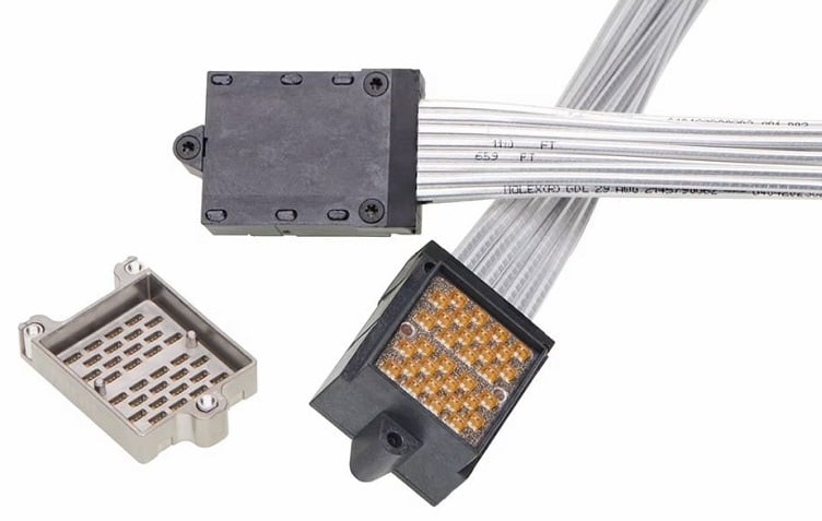
Dies with 224G interfaces will continue to be placed in BGA packages, as is standard for large processors running at high data rates. This is partially due to the lack of any other good approach to package design for modern processors. However, the real strength in these designs is the package ball-out that support 224G signals. These ball-outs have multiple design goals:
- Maintain isolation between multiple 224G lanes to reduce crosstalk.
- Ensure transmission in the TEM mode with a cutoff above 56 GHz.
- Enable impedance matching at the signal launch into the PCB.
These tasks must be successfully completed for the signal to propagate through the package and into the PCB. Similarly, if routing from an interposer through a large substrate to an end package connector, the same tasks apply. The difference is that the signal launch is now on the interposer rather than on the PCB.
At these bandwidths, one of the biggest challenges is designing vias, even when low-loss substrates are used. This is because vias often limit the channel bandwidth when transitioning from the package to the PCB. The problem lies in impedance matching and confining the signal around the via structure. If the vias are not impedance-matched, there will be excessive return loss near the 56 GHz bandwidth, limiting the power that can reach the other end of the channel.
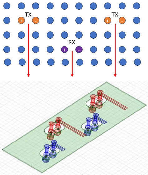 Via arrangements in 224G packages (top view and orthographic perspective view). Head-in-pillow defect. Source: IPC International
Vias are used in both packages and PCBs. Due to the high density of balls and landing pads on the bottom side of these packages, as shown in another article, vias used to reach into the PCB will be stacked, blind and buried vias. This design approach gives the designer a lot of flexibility to land on different layers and tune the via impedance to ensure low return loss.
Package thermal cycling
Packages running these interfaces will generate a significant amount of heat, even with the most efficient designs. Reaching high temperatures is not necessarily a problem; the issues arise from two heat-related factors:
- Stress on copper features during large thermal excursions.
- Repeated expansion and contraction during thermal cycling.
The first issue is being addressed through substrate material selection. Some substrate materials closely match the thermal expansion coefficient (CTE) of copper, ensuring that the copper and substrate expand at approximately the same rate when the package heats up. Excessive stress during heating can cause fractures in certain copper features, most notably small micro-vias. CTE matching reduces the potential for failure. This also addresses the second issue, as thermal cycling imposes repeated expansion and contraction stress on small copper features.
Packaging materials supply chain
Newer materials with CTE matching properties are newer materials without the mature supply chains of earlier organic material sets for packaging and PCBs. The supply chain needs to be considered in the design phase as this will influence product costs and will impact where a design can be produced.
Some of the newer advanced materials targeting Dk less than 3 also possess CTE matching properties. These materials, though costly and with a still-developing supply chain, support signal integrity for components with 224G interfaces. Lower Dk materials allow for slightly larger line widths, which help overcome some of the dominant copper losses observed in return loss spectra for 224G channels.

These materials offer a viable alternative to ABF, which is attractive since most of the advanced materials supply chain is located in Asia. Multinational materials companies are reporting at conferences in 2024 and 2025 that they are working to develop more globalized supply chains to support expected new production capacity in the U.S., Europe and India.
Package and PCB planarity
BGA packages and substrate-like PCBs bonding to mainboards can have a major problem that arises during assembly. During the bonding (reflow) process, the package needs to maintain its planarity so that the bottom-terminated package contacts the PCB. This is an issue in 224G packages due to the very high ball counts required in these packages, which could force the size of the package to be quite large. Reducing the ball pitch in the package helps to reduce planarity problems, but it also requires reducing the ball size, which reduces the tolerance for planarity.
Non-planarity in assembly can create a head-in-pillow defect during soldering, where the package ball does not make sufficient contact with the PCB. The result is an intermittent open circuit failure which is often observed once the package heats up and expands.
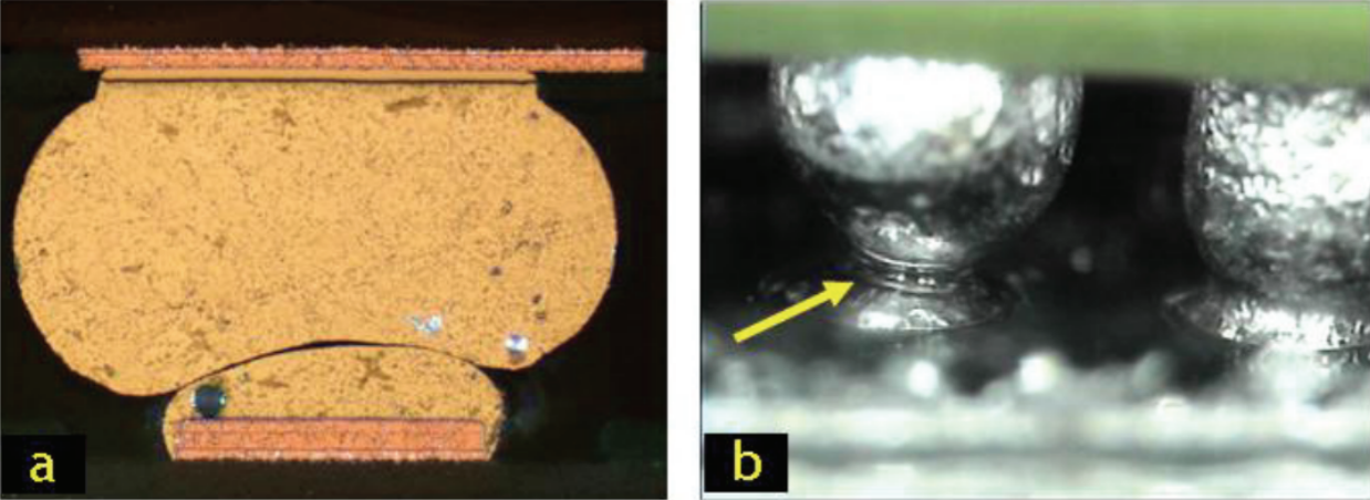 Head-in-pillow defect. Source: IPC International
The non-planarity problem can be reduced with very high-Tg materials, which include newer advanced resin-coated copper materials. However, these materials need to be used on both the PCB and the package to maintain minimal expansion in the ball region. Very high process control and possibly fixation may also be needed during assembly, which then requires the panelized substrates to include appropriate tooling on the panel rails.
