Glass substrates are gaining attention as a structural alternative to organic build-up films/cores in advanced semiconductor packaging. For decades, organic ABF substrates were the dominant material enabling high-density flip-chip and SiP designs. Recently, the buildout of AI accelerators, high-performance compute (HPC) devices, and chiplet-based designs is placing new mechanical and electrical demands on the package substrates.
Many companies producing today’s advanced products have already switched or are looking to switch to glass substrates. This is to support higher I/O density, ensure reliability, control warpage and planarity, and eliminate an interposer in the package. As glass substrates move closer to commercialization, understanding their role helps designers anticipate changes in future component integration.
Scaling pressures in organic substrates
Modern AI and HPC processors rely on extremely large packages that integrate multiple die using 2.5D, 3D and chiplet approaches. Organic substrates, typically built using Ajinomoto build-up film (ABF), provide fine redistribution layers and microvias for routing out of the bump-out. However, as the I/O counts in many processors expanded, pin pitch and bump pitches started to reduce to help keep packages within a reasonable size.
Still, package sizes have expanded over time, to the point where extremely large GPU cards and packages are being deployed in data centers. Traditionally used organic substrates exhibit several characteristics that create reliability challenges in large package sizes:
- Composite organic laminates absorb moisture
- Most composite organic materials have relatively high CTE values compared to copper and silicon
- Stress can occur at copper joints and bumps during high-temperature assembly
- Mismatched (non-symmetric) material stacks can experience warpage
- Large packages experience greater non-planarity compared to the PCB, leading to BGA soldering defects
As die sizes increase and more chiplets are distributed across a large substrate area, warpage becomes more difficult to control in organic substrates. This has led to the search for newer core materials that overcome the warpage challenge.
“Because cores are usually organic materials, they can suffer from high warpage due to the low modulus from their polymeric components,” said Preeya Kuray, post-doctoral researcher at Rutgers University. “One material that has been identified as a next generation alternative to the organic core is glass, which has a high modulus and a low CTE compared to polymer materials. Those characteristics are ideal for preventing warpage of the chip package.”
These mechanical limitations have become more relevant as we began to enter the AI era. While a silicon interposer might normally be used for RDL and fanout routing into die bumps, there are limits on silicon interposer area. Therefore, glass substrates are being evaluated as a replacement for the organic core, which offers the potential for panel-scale manufacturing.
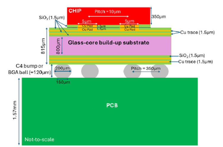 Example glass substrate package design with SiO2 build-up film. Source: IMAPS
What is a glass IC substrate?
A glass substrate replaces the organic laminate core of a package with a sheet of engineered glass. RDLs are fabricated on the surface of the glass, and vertical interconnects are formed using through-glass vias (TGVs). Unlike glass interposers layered on top of organic cores, the glass in this case functions as the primary structural element of the package.
Glass can be engineered with a coefficient of thermal expansion much closer to silicon. It also provides exceptional surface flatness and dimensional stability. These properties allow for tighter lithographic control and improved alignment across large areas, which should result in higher yield during fabrication. In terms of reliability, the closer CTE match to silicon is beneficial if a silicon interposer is used as an integration platform, or when multiple die are attached directly to the built-up film layers.
There are additional benefits for signal integrity in high-speed interconnects. In particular, glass layers exhibit lower Dk value than standard ABF and other organic core materials (such as BT epoxy or other FR4 materials). When combined with some newer advanced chip materials, like thermoset resins and ultra-thin LCP, the entire stack can have Dk less than 3. This is very helpful for expanding channel bandwidths and quasi-TEM limits above 56 GHz, which is a basic requirement for upcoming 448G-PAM6 channels.
Another approach for build-up film fabrication is to use silicon dioxide (SiO2) as the build-up film as it can be grown directly on glass. This effectively allows for etching and metallization to be used for multilayer circuit pattern fabrication, rather than laser drilling and metallization on build-up film layers. This also significantly reduces the misregistration that can result from lamination of an organic build-up film layer on the glass core.

Other aspects of glass versus organic materials
The primary motivation for glass substrates is dimensional stability at large body sizes, but there are multiple aspects that make glass cores a superior option for high-density, high-bandwidth package designs.
For package assembly yield, PCB assembly yield and thermomechanical reliability, the most important factors are the CTE values of the glass materials relative to copper and silicon. Closer CTE matching between silicon and the build-up layer lowers interfacial stress at die attach bumps.
Note that even on glass, organic build-up films are not immune to thermomechanical instability during thermal excursions. According to Gene Weiner, president of Weiner International Associates heat dissipation in organics creates thermomechanical stress, even on glass cores.
“The big problem I see is heat dissipation,” Weiner said. “Every time you use [organic] build-up film, and you try to align it with the next layer, even on glass, as soon as you warm it up or it generates heat, it moves.”
With engineered glass having CTE ~5 ppm/° C and silicon having CTE ~2.5 ppm/° C, thermal reliability could be improved by eliminating the organic build-up films and instead using SiO2. For very large multi-die assemblies, this directly affects long-term reliability under thermal cycling.
Glass substrates represent a structural shift in advanced packaging rather than a minor material update. As AI and HPC devices continue increasing in size, bandwidth and I/O density, substrate mechanics and dielectric performance become limiting factors. Glass cores address warpage, CTE mismatch and dimensional stability challenges while supporting lower-loss interconnects for next-generation channels. Although manufacturing maturity is still evolving, glass substrates are well aligned with the demands of future high-performance package architectures.
