Every so often, the electronics industry runs up against a roadblock that seems insurmountable given the conventional wisdom regarding design and manufacturing. Today, designs with Ethernet channels are nearing that roadblock, specifically regarding implementation of 448 Gbps/lane channels in 3.2 Tb Ethernet. As the major Ethernet standards groups look past the current implementation of 112 Gbps and upcoming 224 Gbps, new questions are arising surrounding the design of these systems for use in data center architecture, particularly for AI compute.
As of early 2025, it appears that the major roadblock to 448G implementation is the PCB or package design. At the most recent SNIA/SFF forum on 400G links for Ethernet channels, I was asked to speak on the topic of extreme SI in PCBs at these data rates, and I was not surprised to see that this was a contentious topic among the attendees. However, it is clear to me that there are a few major challenges that will drive a totally new approach to packages and PCBs if these standard technologies are to enable physical channels at 448G.
The PCB and package roadblock
Many engineers working on data center architecture targeting 448G links remain skeptical as to whether PCBs can be used for signal routing to/from packages and connectors. During my time at the SNIA/SFF event, I heard several objections to routing 448G signals in PCBs:
- Vias in the package ballout will radiate too much energy
- PCB materials are too lossy
- There is no way to overcome copper roughness
These are all valid points, but they do not get to the core issues that impact signal integrity in packages and PCBs. If PCBs are to be used as part of signal routing, there are multiple signal integrity and materials challenges to overcome
First, the modulation format, and thus the required channel bandwidth, are still to be determined. Two modulation options being debated are PAM-6 (86.7 GHz bandwidth) and PAM-8 (74.7 GHz bandwidth). The former is simpler from a circuit design perspective, while the latter is simpler from a PCB/package design perspective.
Secondly, the main signal integrity challenge to overcome in package design, particularly if PCBs will be used to route 448G channels, is bandwidth limiting in the package ballout. Depending on the modulation format and required quasi-TEM bandwidth, package ballouts may need to be smaller than 0.65 mm pitch in order to provide enough margin.
Third, newer advanced materials with zero skew, smooth copper and Dk of approximately 2 are just now reaching the market, and these will be important elements in systems targeting 448G links. These materials are also very thin, which is needed to route transmission lines into BGA packages with 448G interfaces.
The root of the problem
The core problem inherent in routing 448G channels in PCBs is in the via transitions used in BGA escape routing, as well as the signal losses between the package and the connector or transceiver. The bandwidths required in 224G and 448G are so high that this presents design challenges in via transitions:
- The required channel bandwidth will exceed the quasi-TEM cutoff in coarse-pitch BGA packages.
- Via transition produces group delay dispersion at ball pitches above 0.65 mm.
- There is via-to-via crosstalk in denser ball pitches.
There are two great results from Intel’s work for the IEEE 802.3 standards group. Their investigations into 224G packaging also reveal some challenges for 448G packaging. These results are summarized below.
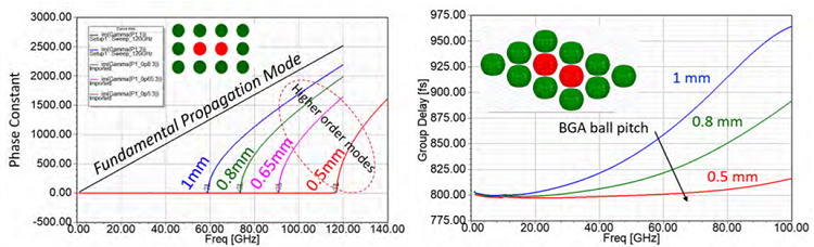 Source: IEEE
Here, we can see that a coarser pitch (0.65 mm to 0.8 mm) may still allow propagation in the quasi-TEM mode, but a denser pitch is required for very low group delay dispersion and this creates a challenge from a crosstalk perspective. In addition, via localization as discussed by Yuriy Shlepnev is very difficult above ~50 GHz, resulting in the possibility of radiation from via structures and thus additional losses.
I have designed some blind/buried via transitions in Dk = 3 materials for 224G-PAM4 channels that exhibit good impedance matching up to approximately 60 GHz, but in those designs, there was little hope of getting beyond the 60 GHz limit. This difficulty in 224G channels is one reason for near-chip and in-package connector architectures as these respectively minimize propagation or eliminate PCB via transitions.
For 448G channels that must interface with a transceiver or connector, there may be another way to build PCBs and packages.
Design paths to 448G
The exact design approach to reach 448G channels in packages and PCBs depends on the modulation format that will enter the new 802.3 standard, which is still undecided as of early 2025. PAM-6 is simpler from a circuit design perspective, but PAM-8 is simpler from the PCB/package design perspective. Both approaches require more bandwidth than the 56 GHz required in 224G-PAM4 interfaces and channels.
At the moment, a variety of simulation data show that PCB via transitions is the major bandwidth limiting element in PCB channels for 448G interfaces. Unfortunately, these transitions are necessary in packages and PCBs, and in particular in BGA escape route for any channel entering the PCB. The difficulties in designing vias to match impedance up to high bandwidths are significant, and there are no good rules of thumb that aid the design process.
With certainty, the solution that extends bandwidth beyond 56 GHz will involve any of the following:
- Smooth copper films, such as through additive processing
- Low-loss surface plating chemistries
- Dielectric build-up film materials with Dk less than 3 and CTE matching to copper
- Fine-pitch BGAs for routing signals into PCBs
- Smaller diameter vias and tighter stitching via arrays
- Skip-layer routing or differential coplanar waveguides
Because vias in these channels are the major bandwidth limiting factor, the vias that make up the package/PCB interface can be eliminated by using substrate-like PCB construction for systems with 448G channels. In a substrate-like PCB, chip-on-board assembly is used to mount high-density packages on an ultra-HDI PCB substrate with a typical IC substrate stackup.
In effect, the PCB is the substrate for the package with the 448G interface, which eliminates the problems with ultra-HDI PCB assembly, dispersion at the package/PCB interface and TEM cutoffs at coarse ball pitches. However, this may pose a challenge with heterogeneous integration in the 448G-capable package, as well as integration of other packages in the same PCB layout.
Conclusion
This was the approach I advocated at the 2025 SNIA/SFF forum on 400G Ethernet links for AI architecture. While it nicely eliminates a major bandwidth limiting element from the design, it requires some qualification by manufacturers to assemble packages onto the substrate-like board. I am confident package designers and PCB designers will be able to converge on the best approach to these types of designs, but time will tell if the newest GPUs and AI accelerators will implement this proposed approach.
