The IEEE 802.3 standard committee has continued to prioritize PAM-4 in networking and data center architecture, with the current fastest data rate being 224G per lane. The next highest data rate might continue to implement PAM-4 modulation, but there are alternative options that could place more focus on things like equalization to ensure data can be recovered from these bitstreams.
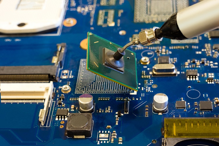
At the center of these systems ensuring 224G channels can operate properly is the physical design of the packaging for these components. Packaging designs and the PCBs where they are assembled are HDI designs with dense, thin interconnects on multiple layers. Even if the PCB is designed perfectly, the packaging will determine whether the channel can operate properly.
224G PAM-4 package characteristics
Components with 224G interfaces rely on vendor IP that implements the interface in silicon. Most often, this is one of a small number of EDA or semiconductor companies, or built custom into the die of a new processor or ASIC. These components are being built as 2.5D or 3D heterogeneously integrated devices in advanced packages, but the package is the critical component that enables the required bandwidth. These components are BGA packages that are bonded to an HDI circuit board with signals routing into the inner layers of the PCB.
The bandwidth in a 224G channel on advanced devices depends on multiple factors related to the component substrate design and packaging. These factors include:
- Pitch between balls on the package
- Vertical routing distance through the package
- Vertical size of skip-layer routing channels
- Dielectric constant of the package substrate
Ball pitch on packages
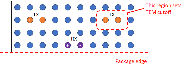
The first major determinant of the bandwidth of a channel in packaging is the ball pitch on the bottom side of the package. When looking at the structure of a set of vias and balls on a BGA package for a 224G-capable component, the structure looks very much like a differential coaxial structure.
This structure with Tx and Rx signals marked on the bottom of the package are shown below. Here, the field needs to be confined around an Rx pair (or Tx pair), and the size of the region sets the TEM mode cutoff.
 Source: Zachariah Peterson
This structure will have some maximum frequency beyond which non-TEM modes will be excited along the axis of the ball/via stack. This is essentially the same effect leading to bandwidth limitation in coax cables, but it involves differential coax signal lines instead of a single coax signal line. Due to potential for non-TEM excitation that limits the TEM mode bandwidth, the recommended ball pitch required to support bandwidths of 56 GHz or higher is not to be larger than 0.8 mm. This means that continued progress into higher bandwidth digital signals requires further scaling downward of ball pitch sizes on devices with 224G PHY IP.
Skip-layer routing
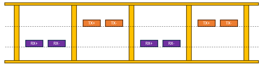
One of the dominant routing methods used to bring signals from a die to the bottom side of the package is skip-layer routing. This type of routing essentially involves striplines staggered on different layers. Using striplines for these routes suppresses differential FEXT but leaves enough flexibility to adjust the dielectric thickness above/below the striplines, which will then adjust the loss in the channel.
The image below shows a cross section of a skip-layer routing, the dashed lines show the dielectric layer interfaces.
 Source: Zachariah Peterson
The skip-layer routing configuration also limits bandwidths in the same way as ball pitch on the bottom of the package. Just as ball pitch (specifically the distance to the surrounding ground balls) determines a non-TEM excitation frequency, the distance to the ground vias and ground references above/below the striplines determines a non-TEM excitation frequency in the stripline structure.
Dielectric constant of substrate
The other factor that impacts the bandwidth of packages is the dielectric constant of the substrate materials. For organic substrates, which are commonly used in IC packages, the dielectric constant can generally range from 3 to 4, although there are materials available with lower or higher values. For example, Ajinomoto buildup film materials used for high-speed IC packages have dielectric constant of 3.2 to 3.4.
The substrate dielectric constant matters because it determines the spatial extent of a signal traveling through a dielectric. When the dielectric constant is smaller, the wavelength of each frequency component in the signal is larger, and therefore signal frequencies need to be higher in order to excite higher-order modes along skip-layer routing and vertical interconnects. This is one reason that high frequency RF designs prefer smaller dielectric constants.
Bandwidth is not the whole story
The other side of bandwidth is losses and the ability to distinguish signal levels above noise. In NRZ bitstreams, even at 56G and 112G, it is much easier to distinguish signal levels because the noise margin is much larger than in a 224G bitstream. The signal integrity requirements at 224G force an interconnect designer to limit channel reach. This could drive a switch from copper cabling (e.g., twinax) reaching a near-chip connector to direct-attach fiber interfaces that are integrated into the package. It remains to be seen if this will drive the next data rate doubling.
