
AI is bringing on a new revolution in computing that demands progressively higher speed links between components in a server, as well as between servers in a data center. Data center architecture and signaling standards have undergone progressive doublings of data rates, which is in line with the trend of Moore's law. High speed serial links have already pushed to 100 Gbps and beyond, and the next round of SerDes channels are targeting 224 Gbps links.
Designing these links correctly, which spans from bumps on a semiconductor die to connectors on a PCB, is influenced by the package format and the fanout routing from the package. The pin placement and ballout used in packaging is a determinant of bandwidth in a channel, simply because the package is a bandwidth-limiting element. How does this arise and what packages will you need for these very fast links? We’ll outline what makes an effective 100 Gbps channel in this short guide.
Factors affecting 100 Gbps and faster channels
When you start to work at these data rates, PCBs and IC substrates in a package start to look very similar. The routing used to guide a signal from a bump into a PCB or onto a module-on-package will be affected by the same small number of factors:
- Dimensions of vias in vertical transitions
- Dielectric constant of the substrate and PCB materials
- Dimensions of ballouts, bump outs and via stitching
- Copper roughness effects
Signals are guided in the substrate plane with skip layer routing, as well as vertically through a package substrate and PCB with vias. Both structures rely on via fences and via stitching to set the channels TEM bandwidth limit to a minimum required value.
Simulation data from Intel as part of the 802.3 working group committee can be used to determine package size limits for 100 Gbps and faster channels. Engineers who are designing their own SiPs with these very high bandwidth channels should understand the packaging design approach and why certain standardized packaging is needed for these transitions.
Packaging ballout
Packages used to support semiconductors with 112 G and faster have some common characteristics, which are summarized in the table below.
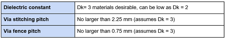
The last two entries in the table can be easily calculated by looking at the wavelength at the channel's Nyquist frequency, assuming 112G and RZ/NRZ signaling or 224G PAM-4 signaling. Both of these signaling formats require the same minimum bandwidth of 56 GHz, and the same design approach is valid for both signaling formats. 112G PAM-4 is also possible and only requires minimum bandwidth of 28 GHz, so a single packaging approach can be used to target all three possible interfaces.
The reason these values listed in the table and above are important is because they relate to the ball pitch requirement on the bottom side of the package. When routing in the substrate, it is desirable to align with the ball pitch because vertical transitions can go directly to the bottom side of the package and deliver a signal to the PCB. The graph below shows the TEM bandwidth limit as a function of ball pitch, assuming the Dk of the substrate material is slightly larger than 3.
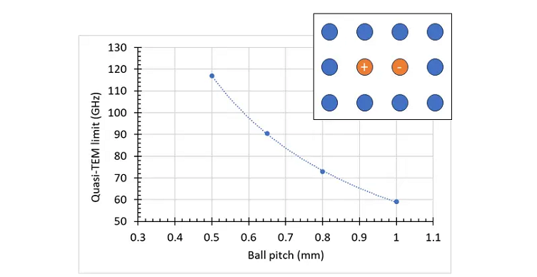 TEM bandwidth limit versus ball pitch for component. Source: IEEE802.org
With a Dk slightly larger than 3, a ball pitch of 1 mm sets a TEM bandwidth limit of 59 GHz. Smaller ball pitches allow for higher TEM bandwidth. This is one of the many reasons that high bandwidth digital channels might require HDI design approaches and finer pitch packaging. While we don't need to go extreme with fine pitch packaging and produce chips with extremely small ball and pad spacing, in general we prefer no larger than 0.8 mm ball pitch for 56 GHz channels.
Group delay dispersion
The other factor that is very important in these channels is group delay dispersion as it provides a measure of signal distortion during propagation. A group delay dispersion curve should ideally be flat across the entire signal bandwidth. In reality, there will always be a little bit of group delay dispersion, but we prefer it to be below some limit.
The graph below shows group delay dispersion expectations up to 56 GHz Nyquist to ensure minimum insertion loss deviation (ILD). Aside from ensuring low ILD, keeping group delay dispersion lower than the edge rate helps ensure minimal edge rate degradation in the channel.
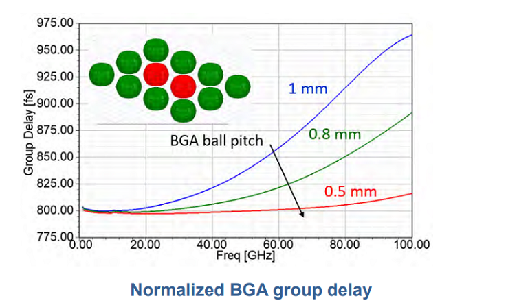 Group delay dispersion versus ball pitch for component packaging. Source: IEEE802.org
The group delay dispersion requirement illustrates the need for consistent dielectric constant and consistent effects of copper roughness in the channel up to at least the Nyquist frequency of 56 GHz. Unfortunately, skin effect varies with the square root of frequency, and variation in skin effect due to copper roughness is an unpredictable function of frequency that depends heavily on the morphology of the copper (see Simonovich for more details).
Because you can never have perfectly smooth copper in these channels, RLCG modeling could be used to determine a desired dielectric constant curve that can compensate for excessive copper roughness and thus produce minimal group delay dispersion. Currently, this is a research opportunity that could allow copper to be used to enable the next data rate doubling beyond 224G PAM-4.
