There is one organic material that dominates the semiconductor packaging market, specifically for advanced packages built on interposers and substrates. That material is Ajinomoto buildup film, or ABF, which is used as a buildup laminate in IC substrates. This material has deserved its success, and with good reason: ABF is a versatile material that comes in thin sheets, and it is compatible with standard additive HDI/UHDI processes. This makes it very useful for fabrication of substrates for integrated circuits up to high layer counts on a central core layer.
Although ABF has proven itself as a reliable material for substrate design, alternatives are on the horizon, both from established companies and startups. Whether one of these alternatives will win out remains to be seen, and it is possible that many advanced chips move completely away from organic substrate materials. We’ll examine the current state of ABF and some alternatives in this article.
ABF material properties
ABF’s material properties help to explain its popularity and usefulness as a package substrate material for integrated circuits. There are multiple material options for ABF available from Ajinomoto, each of which is suitable for high-density, high-layer count substrates and as a buildup film in HDI PCBs. Some material properties values that are most important for packaging are shown below.
These material properties illustrate the desirable electrical performance and reliability of ABF as both a substrate material and PCB material. First, this is a low-Dk buildup film, which requires wider traces in the package to reach a particular impedance value, and thus thinner layers could be used for a given trace width. The material also provides low Df value, and thus low insertion loss, which will minimize losses in the package.
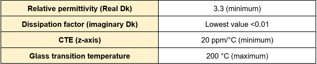
What is often more important for integrated circuit packaging is the Tg and CTE values. The Tg value is quite high, which is compatible with organic materials used as cores in some organic IC substrates, thus we do not have a high temperature region of sudden large deformation in the package. The CTE value is also close to the value of electrodeposited copper foils, additively deposited copper films, and silicon dice. This is important for reliability in packages particularly due to the use of microvias in vertical interconnects in packaging.
Here is a look at some potential alternatives that may emerge in the future.
Thin PTFE films
PTFE-based materials have long been used in RF PCBs thanks to their low loss and very low range of Dk values. In addition, very desirable thermomechanical properties that are comparable to copper are possible in PTFE with ceramic fillers. While PTFE is very useful as an RF PCB material, unreinforced PTFE is very pliable, making it difficult to work with and limiting the thickness value that can be reached.
Very thin PTFE materials have been investigated for some time for use as a buildup layer in RF PCBs with HDI design practices. If thin PTFE with Dk less than 3 can be produced below 100-micron thicknesses, it becomes suitable for use in packaging supporting some of the fastest digital interfaces requiring broad channel bandwidths (e.g., 224G). This area is being investigated by established materials suppliers as they can leverage existing PTFE/ceramics portfolios to fabricate these thin PTFE films.
Isotropic thermoset polymer films
Thin thermoset polymer films are another area of opportunity due to their wide-ranging Dk value, even with the potential to have Dk less than 3. This low Dk direction is very important in more advanced applications involving high-speed serial data lanes, but even more important is the potential for these materials to also be isotropic.
Isotropy in FR4 fiberglass-epoxy materials overcomes an important problem in 10-100 GHz bandwidth ranges: fiber weave effects. This has long been a challenge in PCBs, which has motivated the use of spread glass, and the same strategy can be applied to FR4 cores in packaging. Isotropic films as buildup layers and as a rigid core material can fully eliminate problems with fiber weave effects in conventional materials, such as periodic loading and skew in differential lanes.
Glass substrates
Glass is emerging as a promising material for IC substrates due to its flatness, thermal/thermomechanical properties, and compatibility with high-density fabrication. In terms of reliability, glass has similar CTE value as silicon and copper, so it addresses many of the reliability concerns in advanced packaging. However, there is still very limited reliability data from packages with glass substrates, and this needs to be studied further as glass substrates see greater adoption.
One of the major hurdles with glass substrates is the difficulty in creating multilayer circuits, as current manufacturing processes restrict the number of layers that can be stacked. The transparency of glass also complicates inspection, so new metrology techniques would be required. Despite these challenges, glass is being investigated by companies like Intel and universities as a viable alternative to TSMC’s CoWoS package design, and preliminary work is showing the potential for higher density than CoWoS.
