Silicon, the readily available, inexpensive chemical element that made the computer age possible, is known to be brittle and breakable. This is a problem when it comes to making MEMS, such as the acceleration sensors in today's smartphones. Researchers at ETH in Zurich along with colleagues at the Laboratory for Mechanics of Materials and Nanostructures at Empa have identified conditions under which silicon can be much stronger and more deformable than previously thought.
Over 10 years, lead researcher Jeff Wheeler, senior scientist at ETH's Laboratory for Nanometallurgy, studied how tiny silicon structures deform by looking at the focused ion beam, a common production method. He found that the beam creates surface damage and defects that cause the material to break.
The team then experimented with a type of lithography as an alternative method. The new process involves using a gas plasma to etch away un-masked material from the silicon surface. Next, the surface of the pillars, some narrower than a hundred nanometers, are oxidized and then the oxide layer is removed with a strong acid, explained Ming Chen, a former Ph.D. student in Wheeler's group.
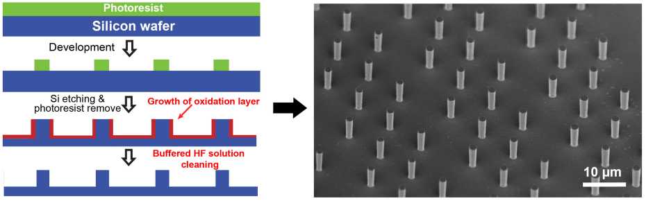 The production process for strong, deformable silicon pillars (links). The pillars are first etched through a resist, then oxidized and finally cleaned. On the right, the end result can be seen (electron microscope image). Source: ETH Zurich
Chen compared the results of the two methods by pressing a tiny diamond punch into each one and using an electron microscope to study their strength and plastic deformability. The pillars milled with an ion beam collapsed at a width of less than half a micrometer. Those produced with lithography had only brittle fractures at widths above four micrometers, and thinner pillars held up to the strain much better. “These lithographic silicon pillars can deform at sizes ten times greater than what we’ve seen in ion beam-machined silicon with the same crystal orientation, with double the strength!” Wheeler summarized. He credits the final cleaning step, which results in the "absolute purity of the surfaces," for the difference.
Wheeler believes that this technique could be used to achieve several benefits, including the ability to make smaller, more robust gyroscopes for smartphones and improving the material's electrical properties for some applications.
The results have been published in the scientific journal Nature Communications.
