An instrument that combines atomic force microscopy (AFM) and scanning near-field optical microscopy (SNOM) enables scientists to visualize matter at a smaller scale than previously possible. Using the instrument, scientists at Brookhaven National Laboratory (BNL) identified previously unknown catastrophic 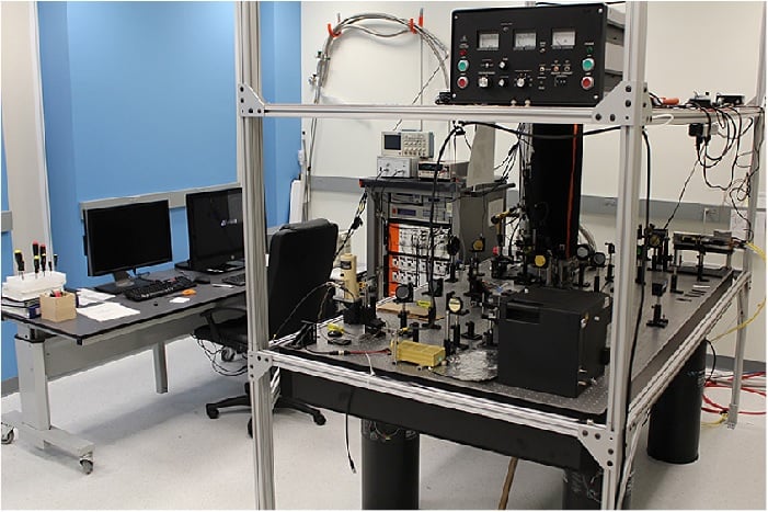 The new instrument, developed at Brookhaven and in use at Yale, combines atomic force microscopy (AFM) and scanning near-field optical microscopy to provide unprecedented insight into these complex nanomaterials. Image credit: Adrian Gozardamage caused by carving nanoscale channels used to create nanowires.
"This is like granting sight to the blind," said researcher Adrian Gozar of Yale University. "We can finally see the all-important variations that dictate functionality at this scale and better explore both cutting-edge electronics and fundamental questions that have persisted for decades."
Scientists from Yale, Harvard, and BNL collaborated to understand why helium-ion beam lithography did not produce the scalable, high-performing superconducting nanowires that theory predicted. Answering this question is of central importance to quantum computing and to companies that are investigating the technology.
The team decided to test helium-beam lithography on LSCO (lanthanum, strontium, copper and oxygen) thin films. In theory, the technique should have produced ultra-thin, precise channels in the film, creating superconducting nanowires.
When their painstaking preparations were unsuccessful, the scientists realized that examining the material directly should answer their questions. Neither AFM nor SNOM could provide a picture at the extreme nanoscale needed.
Gozar created an instrument combining both technologies that “reads” the material’s surface like a needle on a vinyl record. The instrument functions at the cryogenic temperatures necessary for research on these materials.
The “picture” provided revealed that the helium-ion beam wreaked devastating havoc on the LSCO material, creating effects that disturbed atoms far out from the intended 0.5-nanometer beam focus. "Even the slightest nudge at this scale shatters the powerful phenomena we mean to exploit," explained team member Nicholas Litombe. "High-temperature superconductivity can have a coherence distance of just a few atoms, so this lateral effect is devastating.
This new understanding of the effects of forces on these ultra-thin materials opens the door for research into improved etching methods. Gozar’s instrument can be applied to studying other materials at this ultra-small scale.
