Question: What will emerge as the dominant lithography technology in semiconductor manufacturing?
A. 193-nanometer immersion lithography
B. Extreme-ultraviolet lithography
C. Directed self-assembly
D. Nanoimprint lithography
E. Electron-beam direct-write lithography
F. All or most of the above
G. None of the above
Answer: It’s looking like F.
Argon fluoride immersion lithography systems, operating at the 193nm wavelength, are the workhorses of the semiconductor industry. These systems are being used with multipatterning technology, which involves multiple photomasks to produce different layers on a chip, to fabricate devices with ever-shrinking dimensions. Integrated circuit manufacturers are starting to turn out chips with features as small as 10 nanometers.
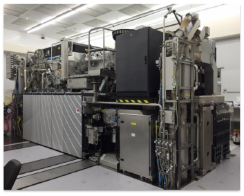 ASML NXE:3350B EUV scanner, the latest model.
Those new parts are typically made with immersion scanners providing the lithographic steps. Meanwhile, research and development continues worldwide on extreme-ultraviolet lithography (EUV), an X-ray-wavelength technology that has been under development for three decades.
Chipmakers have eagerly awaited the advent of EUV for high-volume manufacturing, yet they have been disappointed year after year as the technology has yet to prove its production-worthy readiness.
Intel, the world’s largest chip company measured by annual revenue, has been a big backer of EUV technology, taking an equity stake in ASML Holding, the Dutch company leading the development of EUV scanners, and using ASML’s EUV equipment on its 14nm pilot line. Intel is using Nikon Precision’s ArF immersion systems in its wafer fabrication facilities to turn out its current chip lines.
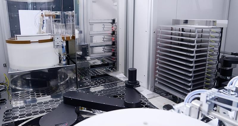 EV Group's HERCULES nanoimprint lithography track system.
EUV scanners have been limited for years by the power available from their laser light sources. ASML set a target of 250 watts for these sources before its scanners could go into volume production of semiconductors. ASML and Intel have reported reaching a power level of 200W, while Samsung Electronics reported the laser on its ASML EUV was able to operate at 80W for eight-plus months.
Toppan Printing, a leading photomask manufacturer, said it has developed a next-generation EUV mask that it will soon sample with semiconductor manufacturers, eyeing full-scale mass production within the next year.
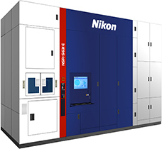 Nikon's new NSR-S631E immersion scanner.
At the recent SPIE Advanced Lithography symposium in San Jose, Calif., attendees heard about the latest developments in deep-ultraviolet and EUV lithography, along with papers on alternative approaches, notably nanoimprint lithography and self-directed assembly. Electron-beam technology has long been used in making photomasks, and the dream of producing chips themselves with electron beams, known as e-beam direct-write or maskless lithography, has existed for many years, with some companies claiming that dream could soon be realized.
Nanoimprint lithography offers a less costly approach, compared with DUV/EUV. Canon Nanotechnologies and EV Group are among the equipment vendors competing in that area. Canon is working closely with Toshiba, one of the world’s largest suppliers of NAND flash memory devices, on developing nanoimprint technology.
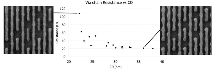 DSA-formed via from Imec.
Directed self-assembly (DSA), considered to be an exotic technology for some time, is getting a closer look by researchers and chipmakers. Belgium-based Imec, an R&D organization, said it was able to form vias for chips with DSA, and sees the potential implementation of via patterning at the 7nm process node. The organization has a templated grapho-epitaxy DSA flow for contact hole shrink and multiplication, which it uses in its 28nm node technology.
“EUV will remain expensive per wafer pass, even at full productivity. Multipatterning will continue to be used,” Mark Phillips, an Intel Fellow, said at a Nikon event held in conjunction with the SPIE conference, Harry Levinson, of GlobalFoundries, said in a keynote address at the SPIE symposium that “EUV lithography does not reduce complexity,” although EUV has the advantage of needing a single mask for exposing the whole chip, as against the three or four masks required for multipatterning. Speaking of the many challenges ahead in lithography, he added, “All of our experience will be needed.”
Richard Gottscho, executive vice president of global products at Lam Research spoke about “Minimizing Process-Induced Variability in Multiple Patterning” during his SPIE keynote. He spoke about the benefits of plasma deposition and etch used in conjunction with lithography, especially with multipatterning. Atomic-level deposition is a tried-and-true production technology, Gottscho noted, and atomic-level etching is coming into its own.
Process variability within dies can be “tuned” through temperature settings, gas flow, and power levels, according to Gottscho.
While new lithography technology was the main topic at the SPIE conference, there were session tracks devoted to metrology, inspection, and process control; patterning materials and processes; and design-process-technology co-optimization for manufacturability, along with advanced etch technology for nanopatterning.
