IBM Research has taken the next step in integrating silicon and optics in the same chip by using a standard CMOS technology to design and test a fully monolithic wavelength-multiplexed silicon photonics chip for 100 Gb/s optical transceivers.
“Making silicon photonics technology ready for widespread commercial use will help the semiconductor industry keep pace with ever-growing demands in computing power driven by big data and cloud services,” says Arvind Krishna, senior vice president and director of IBM Research, in a statement.
IBM’s breakthrough enables different optical components to be integrated side by side with electrical circuits on a single silicon chip using sub-100nm semiconductor technology.
The new chip has speed advantages, potentially of downloading an entire high-definition digital movie in two seconds.
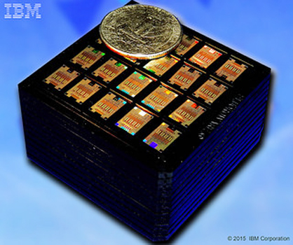 The new chip has speed advantages, potentially of downloading an entire high-definition digital movie in two seconds. Source: IBM
Most of the optical interconnect solutions in data centers are based on vertical cavity surface emitting laser (VCSEL) technology, where the optical signals are transported via multimode optical fiber. The development of cost-effective, single-mode optical interconnect technologies can overcome the bandwidth-distance limitations inherent to multimode VCSEL links.
IBM states its CMOS integrated nanophotonics technology provides an economical solution to extend the reach and data rates of optical links by integrating the electrical and optical parts of an optical transceiver on a silicon chip using a standard silicon chip manufacturing process.
The IBM researchers have demonstrated a reference design targeting data center interconnects with a range up to two kilometers. This chip demonstrates transmission and reception of high-speed data using four laser wavelengths, each operating as an independent 25 Gb/s optical channel. Within a full transceiver design, these four channels can be wavelength-multiplexed on-chip to provide 100 Gb/s aggregate bandwidth over a duplex single-mode fiber, thus minimizing the cost of the installed fiber plant within the data center.
IBM has invested $3 billion over five years in silicon photonics to push the limits of chip technology to meet the emerging demands of cloud and big data systems.
Questions or comments on this story? Contact dylan.mcgrath@ihs.com
Related links:
News articles:
After Apple Win, NXP Gets NFC Deal with Qualcomm
Qualcomm Enters Competitive Fingerprint Sensor Market
The Ramifications of Samsung Using the 14nm Exynos AP in Galaxy S6
