
Flex PCBs, ceramic PCBs, high density PCBs, PTFE PCBs — they all enable a vast set of electronic products we enjoy. There is a more advanced type of PCB that most designers do not work with, but that is equally important in enabling advanced electronics: IC substrates and ultra-high-density PCBs. With PCBs packing more components and features into a compact volume, the interconnect densities in devices increase, and it is to the point now where PCBs are starting to resemble IC substrates.
More OEMs and design teams are bringing packaging design in-house, with design teams starting to build their new products by selecting the appropriate materials. There is some overlap between materials used in ultra-HDI (UHDI) PCBs and those used in packaging. This article will provide an overview on the material options so that designers can make the best decisions for their advanced electronic products.
Packaging and PCBs converge in UHDI
Over the past 20 years, integrated circuit feature sizes, particularly conductors, have scaled downward at an exponential rate due to advances in lithography processes. It has taken significantly longer for the same feature size reduction to be seen in IC substrates and PCBs. The newest and most advanced versions of PCBs, called UHDI or substrate-like PCBs, are starting to resemble integrated circuits as there is now overlap in fabrication processes.
Although integrated circuits are predominantly made from silicon, and other materials like GaAs, or GaN to a lesser extent, the materials used in UHDI PCBs and packaging are also converging with packaging substrates. Materials have to be delineated by composition (epoxy, ceramic, PTFE), target product (UHDI/substrate-like, or substrates) or application area.
UHDI PCB materials
UHDI PCBs will use many of the same materials as standard HDI PCBs. Flexible and rigid materials are available for use in HDI PCBs, with some especially thin materials being used that are not normally found in standard PCBs.
These materials are already widely available and are within the standard processing capabilities of most fabrication houses.
IC substrate materials
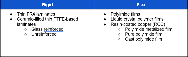
There are three broad classes of IC substrate materials: rigid, flex and ceramic. Some of the popular materials include:
- Rigid — These materials are based on resin systems, such as epoxy resin, bismaleimide triazine (BT) resin or Ajinomoto build-up film resin.
- Flex — Polyimide (Kapton) materials can be used as flexible substrates for IC packaging.
- Ceramics — SiC, alumina or AlN are used in commercially available IC packages.
This is where we see the overlap with standard PCB materials as the list above also appears in standard and specialized PCB designs. Some companies are now making use of PTFE-based materials for use as IC substrate layer buildup films.
Interposer materials
Some newer components are still being built with interposers that use through-silicon vias (TSVs) with stacked dies to provide vertical and horizontal interconnects inside the package. The use of an interposer is not required on all packages, although it is an enabler of 3D heterogeneous packaging used in some of the newest semiconductor products. These devices are now being commercialized for use in high production volume products, such as the newest smartphones.
Interposer materials fall into three possible categories:
- Silicon — These interposers are most common and can be fabricated with active circuitry, an area which is currently seeing significant development.
- Glass interposers — These materials use through-glass vias for vertical interconnects and are entirely insulating.
- Organic materials — These interposer materials have seen a resurgence over the past five years; they are a lower cost option that is suitable for 2.5D packaging.
- Other inorganic materials — Some options include GaAs, GaN, SiC or similarly processable materials.
The range of organic materials is extensive and overlaps with traditional PCB materials. For example, standard FR4 laminates, Rogers PTFE materials, polyimides, or equivalently processable materials can be used for interposers, but they must be available in sufficiently low thickness to enable the required layer count.
Copper foils
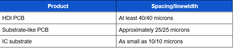
Copper is still the conductor of choice in UHDI PCBs and substrates, but the difference is in how the copper is applied once linewidths and trace pitches get small. At coarse pitch, a photolithography process with laser direct imaging is still useful for exposing a photoresist and etching features into a PCB. The device would then be built up and plated to finish the vertical interconnects. The process is effective for standard HDI boards and has enabled linewidths/spacings down to 40/40 microns.
In substrate-like PCBs and in denser devices, a semi-additive process is used to deposit copper on the substrate layers. Vias are then normally laser-drilled as they would be in HDI PCBs with small linewidth. Semi-additive processing has enabled a further push for linewidths and spacings to even smaller values, reaching as low as 10/10 microns in advanced products.
