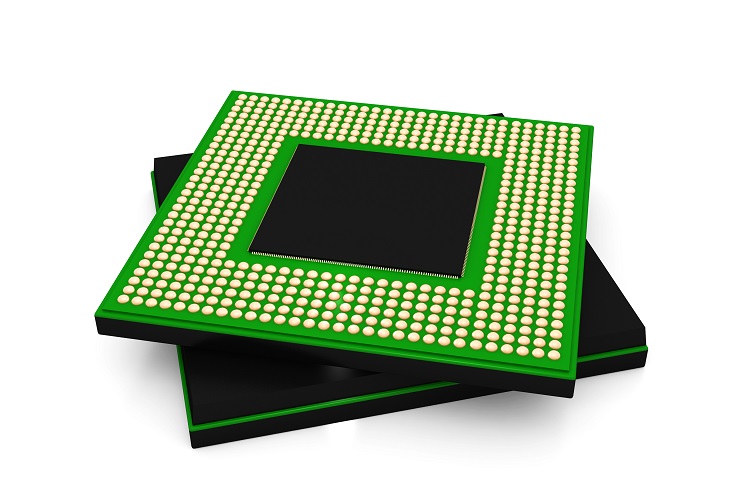
Since IBM and Motorola introduced the first BGA packages in the 1980s, the semiconductor industry has continued to innovate new types of advanced packaging. The major underlying trend in advanced packaging has been integration or packing of more features and circuit blocks into smaller spaces, all operating at faster speeds. To facilitate this type of feature packaging, the industry has developed multiple types of semiconductor packaging designs that enable continued integration of diverse features.
There is real market pressure to pack more functionality into smaller devices, driven by the concept of heterogeneous integration. The IEEE Electronics Packaging Society’s (EPS) Heterogeneous Integration Roadmap outlines a long-term vision for continued integration that is facilitated by advanced packaging. In this article, we’ll look at an overview of packaging options that are driving heterogeneous integration, as well as the consequences for engineers.
Types of advanced packaging
Packaging for semiconductors comes in many varieties. Most designers are familiar with the standard single-die chip or flipchip with wirebonding, which is used in many packages like SOIC or leadless packages like QFN. These standard packaging styles aren’t going away anytime soon as the electronics design and manufacturing industry has come to rely on them so heavily.
Advanced packaging takes an alternative approach, where dies are connected together using a substrate plus interposer structure. The foundational piece that makes advanced semiconductor packaging feasible and economical is the interposer. These thin substrates are the foundation for assembling semiconductor dies with different functions. Each die is then connected with small interconnects, and eventually to the package substrate and the BGA on the bottom side of the package. An example is shown below.
The materials used to build interposers include:
- Silicon — this is probably the most common substrate material used to build interconnects between dies.
- Glass — these interposer materials have become more desirable in advanced products.
- Organic materials — this includes a wide class of materials supporting alternative interconnect fabrication processes.
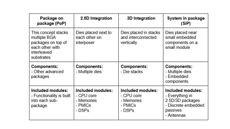
The types of components and their arrangement (2.5D versus 3D) is what is used to categorize different types of advanced semiconductor packaging. The table below summarizes the current set of interposer-based semiconductor packages, as well as some defining characteristics and use cases.
If you’re designing a PCB, you might not know that you are dealing with one of these packages unless you know what to look for. In terms of mounting and assembly, these components are highly standardized and the design practices for placement and routing are well-understood by PCB designers. The major advantages of these packages include the diversity of functions they have enabled in individual components, as well as the overall miniaturization of advanced components.
To date, these advanced packaging options have driven more integration of diverse features into single packages. The end result is the ubiquitous system-on-chip (SoC) or SiP that includes application-specific accelerator blocks on general purpose chips. Some of the newest products from major semiconductor vendors and startups include, for example, FPGA slices or AI accelerator modules alongside a standard MCU architecture. The ability to successfully integrate these features at the package level has even more potential to change how companies design and build components.
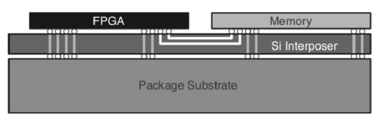 Example package substrate, where an FPGA processor block is integrated in the same package as memory. Source: Xilinx
Democratization of chip design
Perhaps the most interesting shift that could be driven by advanced packaging options is the democratization of chip design. PCB design engineers are well-versed in layout and packaging for standard components, and upon inspection it becomes clear that many of those same skills apply in packaging designs for 2.5D and 3D integrated circuits. The design software used in these applications still requires some productivity boosts, but the workflow would still mirror that used in PCB design.
The fundamental concept is basically the same as in PCB design; the layout engineer builds the interposer substrate to make the required connections on the embedded components and attached dies. The layout engineer only needs to be given pinouts for the attached dies and embedded components. They then use the routing engine in their CAD tool to make the required connections in the interposer and the substrate, and ultimately design the BGA footprint that will attach to a PCB.
Perhaps it’s time for the semiconductor industry to invent a new business model that can support this approach to advanced packaging. This approach to packaging design would be feasible when a layout engineer can choose standardized dies for their new components, rather than a pre-packaged chip that will sit on a PCB. Time will tell if innovators in the industry will step up to build this ecosystem and create the software required to produce these components at scale, but it would expand the role of PCB designers into a new area that gives them more control over the devices they produce.
