Large processors powering today's high-compute applications need a lot of power, something which is no secret even to the layperson. It's not just about the amount of power drawn by these processors; that power also needs to be stable so that the chip does not create excessive noise in a power delivery system during operation. Over time, this has led to continuous innovation in three areas of power system design in motherboards, chip packaging and the chips themselves:
- Placement of regulators for core voltage levels closer to the chips that need them
- Usage of unique materials like ECMs in PCBs and packages to provide power rail capacitance
- Package-level and chip-level power system design to provide stable power delivery
- Development of multiphase power regulator topologies with fast control loop response and higher switching frequencies
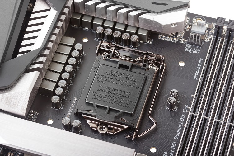
Implementing power regulator solutions has been more difficult for PCB designers, who have been slowly bringing power regulators for core voltages closer to large processors. Unfortunately, PCB designers can only bring their power regulator solutions so close, and at some point, package designers need to take over.
This is where power regulators are being implemented in-package to provide low-inductance power paths for key voltage rails in advanced processors and SoCs/SiPs.
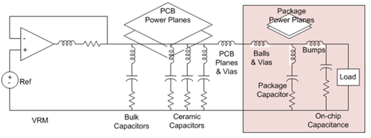
The typical power delivery network (PDN) design
The typical VRM placement around large processors and the resulting power delivery network looks like the images shown below. VRMs are arranged around the chip package on the PCB so that they can provide high power to the core voltage and high-speed I/O supplies. In the circuit diagram below, we see several circuit elements relating to the design of the PCB and the placement of regulators, namely the plane capacitance and plane spreading inductance.
 A diagram of a large CPU with VRMs.
This kind of circuit model can be simulated in SPICE and is typically the systems designer's first stop for estimating the required amount of bulk, decoupling, bypass and plane capacitance in different frequency ranges. Package designers and chip designers can also use this model to determine the amount of in-package capacitance, such as the small chip capacitors, package power-ground plane pairs or on-die capacitance required to achieve a target PDN impedance. Portions of the system design are then typically evaluated post-layout, such as in a 3D electromagnetic simulation.
“Power integrity on the PCB is now demanding a collaborative approach with chip and package designers to ensure stable power delivery,” said Stephen Chavez, principal technical product marketing manager at Siemens Digital Industries. “In the past, PCB designers needed to accommodate whatever capacitance happened to be put on the chip. Now both sides are working together in a silicon-to-systems approach.”
In PDN design, the challenge in ensuring stable power delivery up to progressively higher frequencies is to reduce path inductance, namely the plane spreading inductance defined by the PCB layout itself. Thinner plane pairs and closer placement of key VRMs near processors has helped, leading to multiple approaches to low path inductance power delivery design options:
- Backside or vertical power delivery directly into chip packages
- Active regulator circuit design in-package, specifically in active silicon interposers
- VRM integration on the package substrate
In-package integrated VRM solutions
Integrated VRMs in-package effectively place a VRM component directly on a package substrate, either on the top side with the main ASIC/CPU die or on the bottom side in the ball array area. Some of the new components that have recently hit the market are packaged as highly integrated switching regulators with on-die capacitance in a fine-pitch BGA package. They would then be soldered onto the package using standard reflow soldering.
Conceptually, this looks like the two system architecture options from Empower Semiconductor shown below.
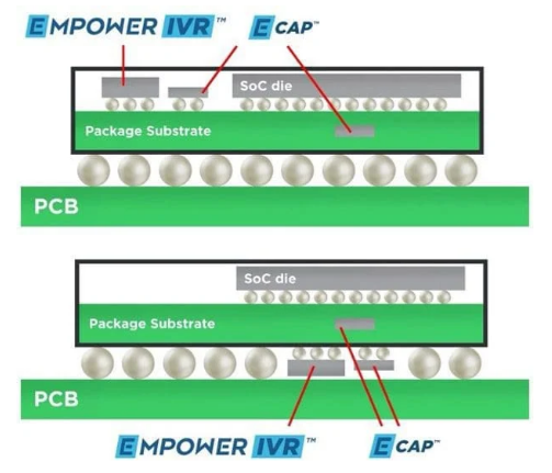 Empower Semiconductor’s diagram of an in-package VRM. Source: Empower Semiconductor
From the PDN impedance standpoint, this is the same as placing a new source of capacitance with low inductance in the 1 GHz range. This fills the gap between the plane spreading inductance, which increases PDN impedance, and the higher frequency range where on-chip capacitance takes over. Integrated voltage regulators can target specific pin groups or rails, such as low-voltage PLL rails, which are used for clocking.
Backside PCB placement versus in-package placement
It is worth asking whether placement on the back side of a PCB is a better option for ensuring power integrity compared to in-package placement. This is worth investigating as it follows the well-known design guidelines of placing capacitance in the PDN close to the digital load as it reduces total path inductance.
Stephen Chavez also notes the trend in power delivery relates to placement of VRMs and capacitors near digital ICs.
“Path inductance has always been one of the big challenges in stable power delivery and in signal integrity,” Chavez said. “If you can find creative ways to reduce that path inductance, then it helps solve some of the simple SI and PI problems. Even though the problem and solution are simple, sometimes it’s tough for a designer to get that part in the perfect location.”
While it may appear that placement of a BGA-packaged VRM on the back side of a PCB reduces total path inductance, there are some disadvantages:
- Placement on the PCB back side requires blind vias routed through the entire PCB thickness, which brings high inductance despite the smaller path length
- The VRM takes up space that would normally be used for decoupling/bypass capacitors requiring low path inductance
- The PCB assembly and inspection process becomes more complex when double-sided BGA placements are used
For these reasons, placement of specific VRMs in-package becomes the best option for reducing path inductance and ensuring lower PDN impedance into the 1 GHz to 10 GHz range.
Looking to the future with chiplets
As the marketplace for chiplets continues to expand and more chiplet-based package design knowledge flows through engineering teams, we may begin to see more chiplet-based power regulator solutions rather than encapsulated modules in BGA packages. The BGA package still has an advantage in that the package can include additional chip capacitance inside the IVR package, something that is often required in small dies with insufficient die capacitance. In the chiplet approach, additional chip capacitors may be needed around the IVR die on the processor package substrate to ensure low PDN impedance.
