
Backside power delivery (BPD) relocates power distribution networks (PDNs) to the underside of semiconductor dies, addressing voltage drop and routing limitations at advanced nodes. While this architectural change offers improvements in power delivery efficiency, it fundamentally disrupts established testing and debugging methodologies that have always relied on backside silicon access.
The dense metallization required for backside power networks blocks traditional failure analysis techniques. As leading semiconductor companies prepare to deploy BPD in production, debug teams must develop new approaches and tools to maintain analysis capabilities within these constraints. As BPD is implemented at the 2 nm node, verification engineers will need to adapt their failure analysis methodologies to work without traditional backside silicon access, potentially requiring new tools and techniques to maintain debug capabilities.
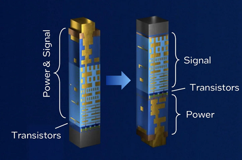
Understanding the shift from frontside to BPD
In conventional semiconductor designs, both power and signal interconnects share the same metal layers above transistors. Power must travel from chip bumps down to the active devices, creating infrared (IR) drop and consuming routing area. This approach has worked for decades but becomes problematic as transistor scaling continues and interconnect resistance increases.
BPD relocates the PDN beneath the transistor layer. Power is delivered through dedicated vias on the chip's backside, which connect directly to transistors. Signal routing remains on the frontside. This architectural change separates power and signal networks, reducing competition for routing area. The result is significant reduction in voltage drop across the PDN and better decoupling at high frequencies. This reduces the demand for on-chip capacitance by reducing total on-chip PDN inductance.
Traditional semiconductor failure analysis relies heavily on accessing the chip through its backside. Engineers routinely thin the silicon substrate and use IR laser probing, focused ion beam (FIB) modifications and optical techniques that require silicon transparency. The backside typically provides the clearest path to isolate and analyze specific transistors or circuit sections.
Because BPD covers the chip's back surface with metal layers and vias, this access is eliminated. The dense backside metallization blocks IR transmission and prevents optical access. In addition, physical modifications with FIB are more difficult due to the presence of backside metallization.
Implementation of BPD requires several new process steps:
- Through-silicon vias must be etched and filled to connect backside metal to transistor power nodes.
- Wafers must go through extreme thinning to less than 100 nanometers, which may require bonding to a carrier wafer for mechanical support.
- The thinned wafer needs to support higher backside metallization to ensure metal lines in the PDN have lower DC resistance.
This briefly summarizes the required fabrication challenges, but components with backside implementation will require verification that relies on new methodologies and tools.
 A lab engineer examines a semiconductor wafer. Backside power delivery could cause issues with wafer bonding through silicon via formal potential defect sources. Source: ryanking999/Adobe Stock
Practical debug solutions
Design teams are incorporating debug-specific structures into their chip architectures. These include dedicated test access points that bypass normal power delivery paths, switchable power domains controllable from external pins and scan chain implementations that provide visibility into internal circuit functions.
A set of backside-focused methods and solutions are being implemented to address the challenges of testing dies with BPD:
- Advanced imaging techniques offer alternatives to traditional optical methods
- Acoustic microscopy can detect voids, cracks or delamination in backside structures
- X-ray computed tomography provides three-dimensional visualization of internal defects
- Lock-in thermography uses electrical stimulus to identify thermal anomalies through the metallization
Process integration considerations
Semiconductor processing now needs to allow room for testing and debug of BPD structure during production. This requires adapting to ultra-thin wafers with backside metallization. Specialized probe cards and handling systems are required to contact delicate structures without causing damage.
 BPD transitions power delivery to the bottom side of the interconnect. Source: Intel/IEEE SpectrumSome debug activities may need to shift from wafer level to package level, where additional access points can be designed into the package structure. This requires coordination between die design and package design teams to ensure debug connectivity is maintained. Test structure placement becomes more constrained and requires careful coordination with power delivery requirements.
Manufacturing and reliability implications
The additional process steps required for BPD create new failure modes that debug teams must understand, and each new process step requires its own monitoring and control methods.
Wafer bonding can introduce voids or delamination. Extreme thinning may cause mechanical stress that affects device characteristics. Through-silicon via formation adds potential defect sources.
The thermal implications of backside metallization also affect debug approaches. Heat generated in transistors during operation must be conducted through the backside metal stack to reach the package thermal interface, and backside methods can interrupt this. The result is new thermal gradients and hot spots that mask the true thermal behavior of the chip/package outside of a testing environment, requiring different measurement and analysis techniques.
Future considerations
As BPD technology matures, new standards and methodologies will emerge. Test equipment vendors are developing specialized tools for BPD-enabled devices, while EDA companies are enhancing design and simulation tools to support verification planning for components with BPD architectures.
The industry's initial implementations will provide valuable learning experiences that inform future design and test strategies, ultimately reducing the time and cost of performing full verification. Success requires preparation in tooling, methodology and team capabilities before the technology reaches volume production.
