Heterogeneous integration, 2.5D and 3D packaging, and chiplets are part of a broader trend in the growth of off-the-board technology, where functionality is steadily moved off of a device’s PCB and into semiconductor packages. This is a natural outgrowth of the broader trend of miniaturization, where higher feature density in components often eliminates the need for external peripherals on the PCB. The growth of packaging technology has taken this to new levels in some of the most advanced components, such as high-speed network ASICs, AI accelerators and GPUs.
Off-the-board technology has proceeded in three waves, and the third wave is still unfolding. Based on the author’s experience working with startups, the third wave may coincide with the end of copper interconnects for the fastest digital interfaces and a shift to optical interconnects with silicon photonics for on-chip processing. This transformation will fundamentally reshape how we design high-performance computing systems and could unlock performance levels that are simply impossible with traditional electrical approaches.
The old days of SiP and SoM
Off-the-board technology has come in waves and is evolving to meet key needs for more advanced electronics. Many PCB designers are familiar with SiP and SoM components, which provide a highly integrated solution on an organic material platform that can be placed into standard PCB assembly processing. These approaches to component design offered manufacturers a new way to integrate multiple system functions into a single package with cost-effective manufacturing, ushering in the first wave of off-the-board technology.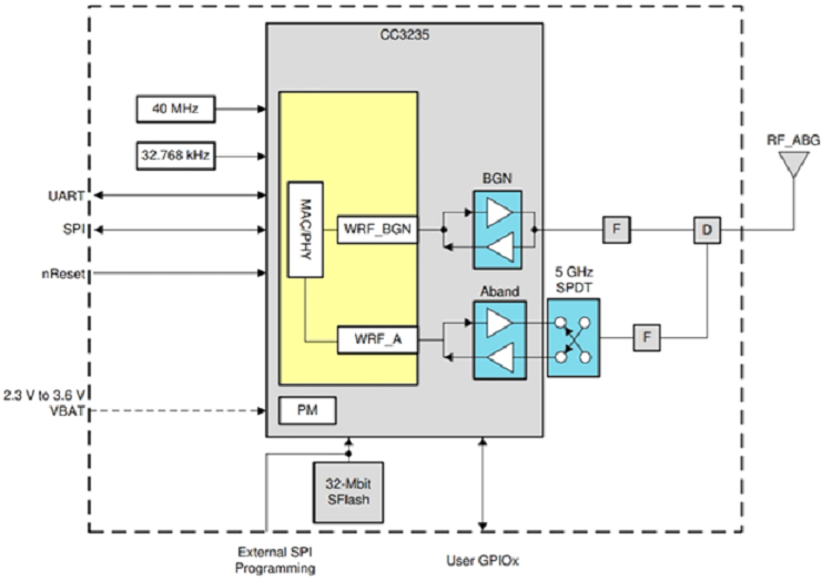 An example of the SoM block diagram for the CC3235MODSF MCU module. Source: Texas Instruments
SoMs are components that integrate a single die or packaged component, as well as peripherals and passives, into a single package. While some SoMs still connect to the main PCB through a connector, the most popular SoMs are in LGA or castellated packages, which can be reflow or hot-air soldered onto a PCB.
SiP also changed the industry by enabling the integration of multiple semiconductor dies into a single package. Rather than mounting individual components across a PCB's surface, component engineers can combine analog, digital, RF and mixed-signal functions into a compact package. Multiple dies can still be combined with packaged components or off-the-shelf discrete/passive components.
Key advantages of SiP technology:
- Reduced board space by eliminating redundant packaging
- Improved signal integrity through shorter interconnects
- Better thermal management with integrated heat dissipation
- Lower package assembly costs
- More diverse feature integration
Both approaches brought complete functional subsystems, including processors, memory, power management and I/O interfaces, into standardized modules and pulled many of these functions off the PCB. The cost-effectiveness of these early off-the-board technologies stemmed from their ability to repurpose existing semiconductor dies and off-the-shelf ICs into new components. Rather than designing every application processor from scratch as custom silicon, manufacturers could combine proven components and focus on design of the component substrate. This approach also enabled smaller companies to compete with larger players by accessing advanced functionality without the high costs of custom chip development.
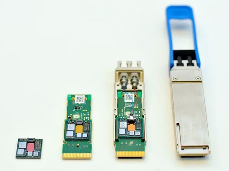
 A development kit or packaged board interfacing silicon photonics dielets to fiber arrays, designed for prototyping. Source: Phix
Off-the-board technology in 2.5D and 3D packaging
The evolution of off-the-board technology has accelerated dramatically in terms of feature density and capability with the advent of advanced 2.5D and 3D packaging technologies. These sophisticated approaches are moving more critical system components off the traditional PCB and into the integrated circuit package itself, representing a significant leap forward from the early SiP and SoM implementations.
In 2.5D packaging, memory subsystems are increasingly being integrated directly into the package alongside the main processor. HBM stacks are the best-known component following this trend, where multiple memory dies are stacked vertically and connected to the processor using micro-bumps and through-silicon vias (TSVs). This integration eliminates the need for external memory modules on the PCB, significantly reducing signal path lengths for high bandwidth memory channels.
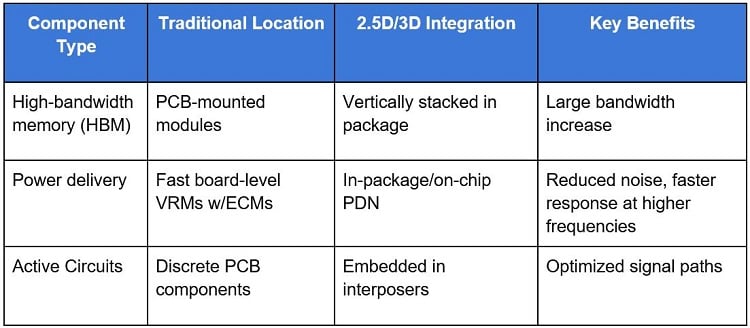
PDN design has also received more attention as an off-the-board, illustrating the trend of considering power integrity holistically, spanning from the PCB and onto the chip. VRMs are still located on the PCB but are accompanied by a purposefully engineered in-package PDN and on-chip capacitance. Focusing more on the package and chip PDN alongside PCB PDN design is a requirement to ensure power integrity out to very high bandwidths, something that is required in today’s fastest digital processors.
Silicon photonics: The next wave of off-the-board technology
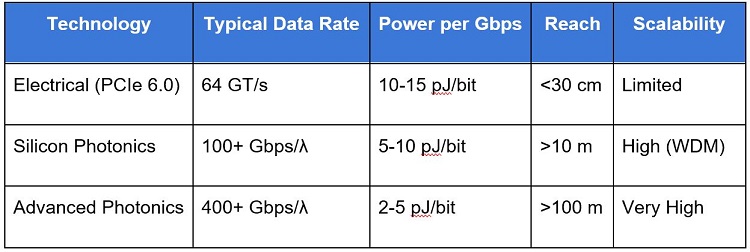
Growth in 2.5D and 3D packaging solutions has accelerated off-the-board technology and the components which leverage it, both in terms of the fastest digital processors but also in proprietary ASICs and application processors. As high-bandwidth digital channels approach the practical limits of copper interconnects, silicon photonics and on-PCB/in-package optical interconnects may emerge as the next transformative wave of off-the-board technology.
This opinion is shared by insiders within the PCB and packaging side of the industry
“Off the board technology is growing at an amazing rate, and isn't being replaced by optical solutions, it's enabling more optical solutions,” said Joe Dickson, senior VP chip-to-chip reliability and innovation at WUS PCB International. “They are not competition, they are tools to go much farther than we can today.”
Silicon photonics leverages mature silicon manufacturing to create optical processors that can be integrated directly with electronic circuits. Unlike traditional optical transceivers that require separate discrete components and often use compound semiconductors (III-V and II-VI), silicon photonic devices can be manufactured using standard CMOS fabrication techniques. This compatibility enables pulling optical transceiver and processing functions off the PCB and integrating them directly into semiconductor packages.
While electrical signals face increasing challenges at high frequencies due to skin effect losses, dielectric losses and EMI, optical signals can maintain excellent signal integrity across much broader bandwidths and in multiple propagation modes. Silicon photonic links can potentially support data rates of hundreds of gigabits per second per channel, far exceeding what's practical with electrical connections.
On paper, this looks like the most obvious approach for super-fast digital systems and packages, but integration of photonics between chips, packages and PCBs requires a totally new approach to integrate optical interconnects in traditional substrates. Currently, companies working toward production-grade silicon photonics devices are still relying on flyover optical fiber attached to a silicon optical interface in order to send and receive data between chips. Commercialization of optical interconnect technologies in PCBs and packages is one area that deserves its own article and which I may address in the near future.
