
Power integrity in modern electronic systems extends far beyond traditional bypass capacitor placement and power supply design. As processors demand higher performance and digital interfaces push into multi-GHz frequencies, maintaining stable voltage delivery requires a comprehensive system-level approach that integrates the PCB power distribution network (PDN), chip package design, on-die capacitance and VRM control characteristics.
For modern PCB and package designs, a system-level approach is needed.
Power integrity at the system level
Before new designers get a full understanding of power integrity requirements in PCBs and packages, their focus is most often on power supply design, placement of bypass capacitors, and placement of decoupling capacitors. For large processors with fast digital interfaces and for substrate designers working on packages for large processors, the power integrity requirements span beyond selection and placement of discrete capacitors:
- The voltage ripple must be within limits as measured at the die’s supply bumps
- Fast digital designs require low PDN impedance in the PCB and package
- VRMs for large processors must have sufficiently fast control loop response
Voltage ripple at the die pin
Because the range where low PDN impedance is required has extended to higher frequencies, designers should not assume the package and die can overcome high inductance in the PDN on the PCB. The PCB and packaging must work together to provide stable power in large processors to ensure the voltage ripple observed at the die pin falls within the compliance limit specified by IP vendors. This applies in packaging for custom chips, chiplet-based designs and 2.5D/3D packages.
"Most of the IP vendors and ASIC designers that are making these pieces of IP are specifying the compliance point from a voltage perspective to the die bumps," said Ben Dannan, founder of Signal Edge Solutions. So if you're designing a substrate or a package, you need to understand how to model it to the die bumps.
This means the PCB designer needs to include information about the chip package and die in their simulation package in order to verify power integrity is achieved at the die bump. The same idea applies to chip/package designers but in reverse; the designer needs to ensure they provide enough in-package/on-chip capacitance required for the PCB plus package system to hit the PDN impedance target and thus stay within the voltage ripple limits as measured at the die bump.
Unfortunately, the die capacitance needs to be correct, otherwise the voltage ripple seen at the die bump will be overestimated. Furthermore, there will be no way to meet the ripple spec from the IP vendor, especially because adding more discrete or plane capacitance stops working at some point.
"The die capacitance needs to be correct because not only does it impact your ripple, it also impacts your jitter," Dannon said. "But there's a limit on how much on-package capacitance you can have; adding more discrete capacitance eventually stops working and there's a point where ripple can only be reduced by adding more die capacitance."
PDN impedance
As I/O speeds have increased, the frequency range where PDN impedance must be low has also increased to support the broader channel bandwidths required for high-speed signals. During simulation, the PCB designer’s job is to ensure the level of decoupling/bypassing and plane capacitance on the PCB works together with the chip plus package capacitance to extend the low PDN impedance range into GHz frequencies. A low PDN impedance throughout the relevant frequency range helps ensure low voltage transients would be seen in the time domain.
A typical SPICE model encompassing the PCB and package is shown below. Circuit models are very useful for qualifying whether capacitance in the PCB and package PDN is sufficient to overcome inductance in the layout, but only in cases where these estimates are accurate. These values are also critical to get correct due to the inductance in the system.
"You can have the perfect package in the world, but you're always going to have inductance that you're going to be fighting against," Dannon said.
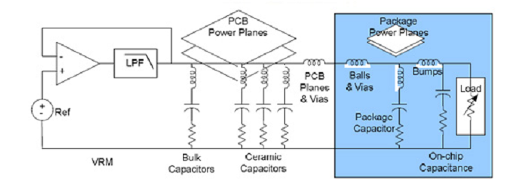 Typical PDN model encompassing the PCB and package. Source: Steve Sandler/Signal Integrity Journal
Estimates of capacitance and inductance often lead to an underestimation of the PDN impedance, with the result being that voltage ripple is higher than expected. 3D electromagnetic simulations are often needed to validate power integrity in a typical PCB layout and package layout, which can help validate the parasitic capacitance and inductance estimates in the system. This is necessary due to the complex geometries in these systems, where inductance and capacitance will arise in any of the following features:
- Power/ground plane pairs
- SMD component footprints
- Vias and traces connecting SMD components
- Pin-package inductance from BGA balls and die bumps
Complexity in these systems requires engineers to better understand and use 3D field solvers to validate power integrity, which is a challenge EDA tools are helping address.
VRM control loop
The VRM control loop plays a critical role in maintaining stable power delivery to high-performance processors, but its effectiveness becomes increasingly challenged as load transient speeds approach the control loop bandwidth limits. Modern processors can generate load transients with di/dt rates exceeding 1,000 A/μs, creating voltage perturbations that the VRM must respond to within its bandwidth constraints.
VRM control loops typically operate with bandwidths ranging from 10 kHz to 100 kHz, depending on the switching frequency and compensation network design. Above this bandwidth, the VRM cannot actively regulate voltage fluctuations, making the passive PDN elements responsible for maintaining low voltage ripple. This creates a critical handoff frequency where VRM regulation transitions to passive PDN response.
The challenge intensifies faster digital interfaces requiring multi-GHz channel bandwidths. Load transients from these high-speed circuits occur at frequencies well beyond typical VRM bandwidth, meaning the entire burden of voltage regulation falls on the capacitive elements in the PDN. This is why achieving low PDN impedance across the frequency spectrum becomes essential: the VRM cannot compensate for inadequate passive components at high frequencies.
Conclusion
Successfully achieving power integrity in modern high-performance systems requires abandoning traditional compartmentalized design approaches. Engineers must consider the entire power delivery path from VRM output to die bump as an integrated system. The frequency-dependent handoff between active VRM regulation and passive PDN response creates design interdependencies that demand comprehensive modeling with accurate parasitic estimation. EDA tools are evolving to support this need, and better vendor support for die modeling will help ensure simulations more closely correspond to reality.
