
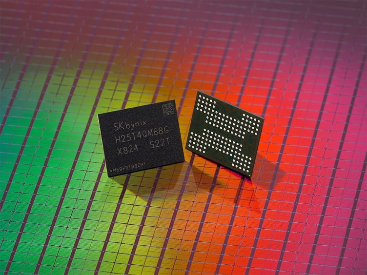
Korean memory maker SK Hynix Inc. has entered volume production of what it claims is the world’s first QLC NAND flash with more than 300 layers.
Inside the 321-layer 2 TB QLC NAND flash, SK Hynix increased the number of planes and independent operation units within the chip from four to six to enable greater parallel processing and enhance simultaneous read performance.
Because of this, the 321-layer QLC NAND has a higher capacity and an improved performance compared to other QLC products, SK Hynix said. Additionally, the NAND flash features:
- Double data transfer speed
- 56% improved writer performance
- 18% improved read performance
- 23% increased write power efficiency
SK Hynix said it plans to first apply the NAND flash to PC solid-state drives (SSDs) before expanding it to enterprise SSDs for data centers and UFS for smartphones.
“With the start of mass production, we have significantly strengthened our high-capacity product portfolio and secured cost competitiveness,” said Jeong Woopyo, head of NAND Development at SK Hynix. “We will make a major leap forward as a full-stack AI memory provider, in line with the explosive growth in AI demand and high-performance requirements in the data center market.”
