The utility of consumer flatbed scanners in gauging the optical properties of solar cells was demonstrated by researchers from the University of New South Wales and Macquarie University, Australia. These low-cost devices may offer results comparable to those of high-end tools used in the photovoltaic industry for some types of cells and wafers.
A contact image sensor (CIS) scanner, which works by being almost in direct contact with the object to be scanned, was used to monitor the spatial variation in the texture of multi-crystalline and mono-crystalline wafers prepared with varying texture conditions. Its performance was compared to that of the Loana system commonly utilized in the solar industry and at the research level.
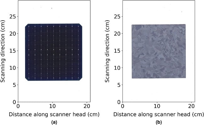 Example scan of (a) a silicon solar cell from a 2020 manufacturing line and (b) textured multi-crystalline wafer used in this study. The scan has 118 pixels per cm and was taken with a CIS based Canon Lide 300. Source: Macquarie University/Scientific Reports/CC BY 4.0
The researchers observed good correlation for all metrics for the multi-crystalline wafers of varying textures. The results published in Scientific Reports confirm that the low-cost CIS scanner technology is suitable for monitoring polycrystalline devices, although they do not extend to monocrystalline wafers. The scanner did not adequately capture the reflection of the random pyramid texture caused by the alkaline texturing process.
