Years of continued U.S. and European export restrictions were designed to slow China’s growth in semiconductor manufacturing.
In some ways, they have. Advanced node production remains constrained and the lithography bottleneck from not having access to The Netherlands’ ASML cutting edge tools isn’t going to resolve soon.
But, on the other hand, the export restrictions have had an unintended effect: China’s domestic push to build its semiconductor ecosystem from the ground up.
That includes developing domestically made state-of-the-art chips, semiconductor equipment and advanced packaging.
Advanced nodes still impacted
No doubt China’s production capacity in the advanced process nodes remains significantly impacted by equipment export controls, according to market research firm TrendForce.
According to Joanne Chiang, analyst at TrendForce, near-term breakthroughs are unlikely, but over the next five years, domestic Chinese semiconductor manufacturing will get better and bigger.
“Rather than a sudden leap into leading-edge nodes, we expect a period of steady, incremental optimization of the domestic supply chain,” Chiang said.
In this timeframe, China will focus on three areas:
- Stability testing
- Capacity expansion
- Yield improvement
The testing will focus on validating reliability of domestic equipment in live production environments. China will also scale up production lines in mature and legacy nodes that are still used across a wide range of applications. Finally, China chipmakers will look to close the efficiency gap to make domestic tools more commercially viable and improve yields.
Closing the chip gap
In April of 2026, Shanghai startup Dishan Technology said it had made significant progress in developing 2 nm AI chips and was currently in the prototype verification stage. Dishan’s chip has not yet reached the tapeout stage, but it plans for commercial deployment between late 2028 and 2029.
Additionally, Chinese smartphone and equipment maker Huawei announced it was developing advanced semiconductors despite U.S. export restrictions. The company developed an engineering approach called “LogicFolding” to manufacture its Kirin smartphone chips.
Purportedly, Huawei’s Mate 60 smartphone included 5G connectivity through an advanced in-house chip it developed to regain market share it lost due to export restrictions.
Huawei said the chip technology could deliver capabilities equal to 1.4 nm process technology. Huawei is aiming for commercialization of the chip by 2031.
While these chips could position Dishan as a global AI chip leader and push Huawei back into a leading smartphone position, it may be difficult to find a domestic foundry capable of turning the design into commercial chips, TrendForce said.
Cut off from some important advanced semiconductor equipment and advanced tools from the U.S. and Europe, China is turning internally to develop its advanced processing equipment and tools.
Equipment developments
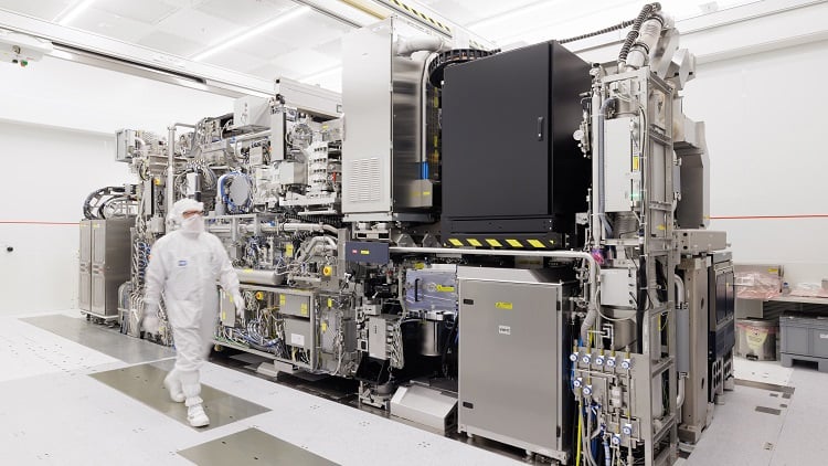
One of the main focuses of the export restrictions is on semiconductor equipment. China has been restricted through exports to get its hands on advanced semiconductor equipment and tools to push its own technological improvements in its chip fabs. This is specifically troublesome with advanced lithography tools.
Because of this, China has been aggressively pursuing localization across various sectors like semiconductor equipment, chemicals/raw materials, wafer manufacturing and advanced packaging.
“While progress in precision technologies, specifically wafer manufacturing and advanced packaging, has been hindered by international equipment export controls, China has secured significant global standing in several other fields,” Joanna Chiao, analyst for market research firm TrendForce, told Electronics360.
Over the past five years, China’s equipment strategy has been twofold: strategic stockpiling and domestic R&D.
First, China has made large-scale purchases from international equipment giants to prevent disruptions in wafer manufacturing and packaging R&D. Second Chinese equipment makers have funneled massive capital into R&D and production over the last decade.
This R&D has resulted in technical breakthroughs and growth in etching, cleaning and CMP, Chiao said.
“Despite these advancements, the most significant bottleneck remains lithography,” Chiao said. “This area continues to be the primary hurdle preventing China from achieving full self-sufficiency in high-end chip production.”
China’s largest foundry, Semiconductor Manufacturing International Corporation (SMIC), has been able to push their old equipment to the limit but yields are getting worse as SMIC pushes to quadruple patterning. China is seeking to enable smaller advanced nodes without having the proper equipment from ASML and others.
However, in November of 2025, researchers at Peking University in China developed a lithography advancement that uses cryo-electron tomography (cryo-ET) to visualize, for the first time, in-situ 3D microstructure, interfacial distribution and entanglement behavior of photoresist molecules in a liquid environment.
Deals incoming?
In early July 2025, the U.S. government struck a deal with China that eliminated restrictions on U.S.-based electronic design automation (EDA) firms — like Synopsys, Siemens EDA and Cadence — sending technology to the country.
In exchange, China curbed some export controls on rare Earth materials like antimony, gallium and germanium.
Other deals could come as the U.S. seeks to retain materials for its own semiconductor supply chain. More fuel to this possibility came after President Trump’s trip to China in May where he brought 17 U.S. CEOs —including Apple’s Tim Cook, Tesla’s Elon Musk and Nvidia’s Jensen Huang — for meetings with Chinese officials over potential future tech deals.
Domestic tools rising
While the EDA tools are a boon for Chinese foundries and chipmakers, Chinese-made tools are also gaining traction, particularly domestic tools for testing and validation.
Tools for etching, PVD/CVD and cleaning have achieved the most effective penetration into domestic Chinese semiconductor production lines, TrendForce said. However, it varies significantly depending on the specific fab and technological requirements.
Chiang said that China is effectively driving localization by linking fab permits to equipment usage with authorities requiring new wafer fabs to meet a specific minimum threshold for domestic equipment adoption before granting construction licenses.
“Moving forward, any new fab projects are expected to be subject to strict regulatory frameworks regarding the proportion of domestic machinery used,” Chiang said.
Not just state backed
For years, the domestic Chinese semiconductor push has been driven by state-back initiatives to compete. But the country’s chip race may no longer just be solely backed by the government as major Chinese vendors are now advancing their own semiconductor development across different sectors.
This includes Xiaomi, BYD and NIO that are now driving certain chip manufacturing in the country.
For Xiaomi it comes down to defining its own smartphone path. Caught between using MediaTek or Qualcomm for its main applications/baseband processor, the company is looking to drive its own investment into smartphone system-on-chips through new chip investment.
At BYD, the company is seeking to develop IGBTs and silicon carbide (SiC) devices due to the volatility in the wide bandgap chip market and overall power semiconductor sector. BYD now has an operational SiC production line to develop chips for its electric vehicle fleets.
For NIO, the volatility in the automotive chip market is leading to the company developing its own chips for autonomous driving.
