This week’s online Technology Symposium and Open Innovation Platform (OIP) Ecosystem Forum hosted by Taiwan Semiconductor Manufacturing Corp. (TSMC) brought together people worldwide to give a preview of the latest technology offerings from the world’s largest semiconductor foundry.
The conference, held virtually, is designed to focus on the pure play foundry’s next generation moves as well as what its partners are doing to help support the current and future process technology including electronic design automation giant Synopsys and infrastructure partner Marvell.
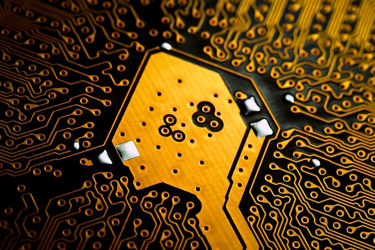
Advanced process technology
During the event, TSMC detailed its move to 5 nm (N5) process technology, which entered into volume production this year, and how defect density reduction is proceeding faster than previous generations. N5 provides a 15% performance gain or a 30% power reduction as well as up to 80% logic density gain over preceding N7 technology. The company said it plans to ramp an enhanced version of N5 in 2021, called the N5P.
TSMC detailed its next generation 4 nm and 3 nm technology. N4 (4 nm process technology) will provide improvements in performance, power and density as well as a migration path with the ability to leverage the 5 nm design ecosystem. The N4 process is scheduled to start risk production in the fourth quarter of 2021 with volume production scheduled for 2022.
Meanwhile, the 3 nm process technology is on track to become the most advanced logic technology worldwide with a 15% performance gain, up to 30% power reduction and a logic density gain up to 70% over N5. TSMC did not give a time frame for when N3 might be available.
Synopsys announced it has certified its digital and custom design platforms for TSMC’s 3 nm process technology. The certification is based on TSMC’s design rule manual and process design kits and is an extensive collaboration to deliver design solutions for optimized power, performance and area.
5G and IoT
During the event, TSMC introduced a new process, called N12e, which is optimized for edge artificial intelligence (AI) applications and brings FinFET transistor technology to edge devices enhanced with ultra-low leakage and static random-access memory (SRAM) to deliver more than 1.75 times logic density improvement and about 1.5 times performance improvement, TSMC said. The N12e process is designed for internet of things (IoT) devices running on 5G and powered by AI.
Extension of Marvell partnership
Marvell and TSMC have extended their partnership to advance essential technology for infrastructure to provide the storage, bandwidth, speed and intelligence for the next generation digital economy. The deal will allow Marvell to manufacture silicon on TSMC’s 5 nm portfolio and its IP portfolio will cover a full spectrum of infrastructure requirements including high-speed SerDes up to 112 Gbps long-reach, process subsystems, encryption engines, system-on-chip fabrics, chip-to-chip interconnects and a variety of physical layer interfaces.
The technologies are in development on TSMC’s N5P process, which is said to provide about 30% faster speed and 40% power reduction compared to the previous 7 nm generation. Marvell said under the extension it is developing solutions across carrier, enterprise, automotive and data center markets with product sampling by the end of next year.
3DFabric
During the OIP event, TSMC introduced 3DFabric, a system created via robust chip interconnections. This technology offers an array of options for both silicon stacking at the front end and packaging chips together at the back end. 3DFabric allows companies to connect logic dies together, to high-bandwidth memory or to chiplets such as analog, I/O and RF blocks.
Additionally, TSMC claims the technology is the first solution to combine back-end 3D and front-end 3D technologies for a multiplier effect in system integration. The technology also augments and complements transistor scaling for improving system performance, functionality, slimming form factors and improved time-to-market.
