Taiwan Semiconductor Manufacturing Co. (TSMC) has successfully entered volume production of 3 nm process — technology that will create devices serving $1.5 trillion in value inside five years.
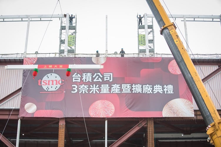
The announcement was made at a ceremony at TSMC’s Fab 18, currently under construction in the Southern Taiwan Science Park, which will produce both 5 nm and 3 nm process technology.
Phase 1 through 8 of TSMC’s Fab 18 will have a cleanroom area of 58,000 square meters, about double the size of a standard logic fab. TSCM is investing more than $60 billion in Fab 18 which will become a gigafab and create 23,500 construction jobs and more than 11,300 direct high-tech jobs.
TSMC is also building 3 nm capacity at its upcoming Arizona fab, which is currently under construction. TSMC recently announced it would build a second fab in Arizona next to the current facility, which is also now under construction.
The company said it is using water resources from the TSMC reclaimed water plant to reach a target of using 60% reclaimed water by 2030. It is also doing this at its Arizona fabs. Once volume production begins at Fab 18, it will use 20% renewable energy to reach the sustainability goal of 100% renewable energy and zero emissions by 2050.
The 3 nm process is a semiconductor technology in both power, performance and area and in transistor technology. It is a full-node advancement from the 5 nm generation. TSMC said compared to 5 nm, 3 nm offers up to 1.6 times logic density gain and 30% to 35% power reduction at the same speed.
