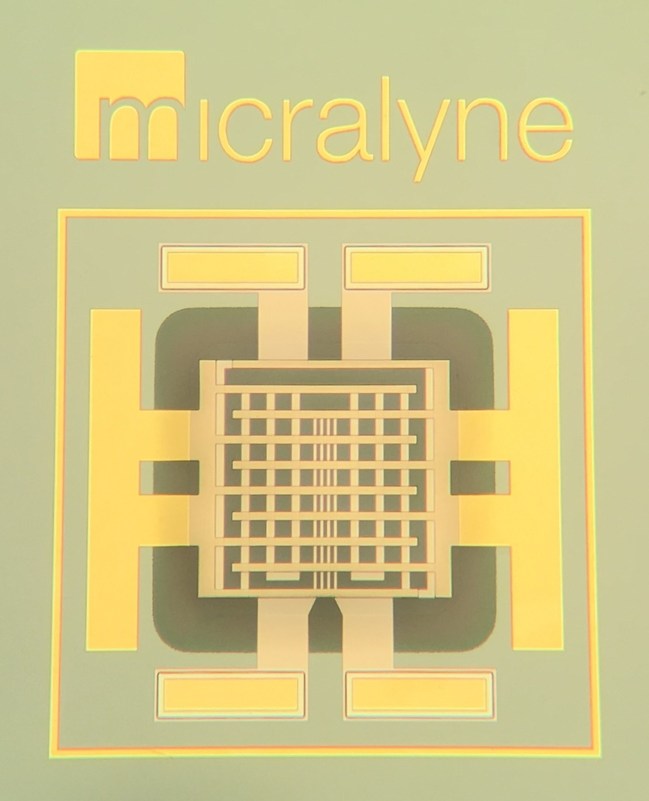
 metal oxide gas sensor with integrated micro hotplate, 1.6-by-1.6 millimeter die size. (Source: Micralyne)
Micralyne Inc. has teamed up with Microplex in Placentia, California to develop and manufacture custom wafers with metal 'through silicon vias' (TSVs). The development of this technology uses the expertise of both companies to develop a flexible and cost effective Metal TSV solution for sensor and semiconductor applications. Both of the companies engaged in the TSV development in 2016, and full production starts in July 2017.
The companies joined together to deliver standalone TSV wafers and an integrated TSV solution with metal layers for interposer and redistribution layers. Micralyne offers multiplayer wafer level packaging (WLP) with metal TSV technologies for ball-grid-array sensors.
The minimum hole diameters currently being created are 40 and 70 micrometers. The diameter to depth ratio of the via holes can exceed a ratio of 20-to-1. This provides a flexible and robust wafer thickness. Conductive via fills come in gold, silver and copper. According to Micralyne the wafers are optimized with processing and unique formulations that ensure effective performance with high-frequency device applications all while maintaining the purity of base silicon microstructures.
To learn more about these wafers, visit the Micralyne site here.
