For decades, semiconductor innovation has focused on shrinking transistors. But in emerging devices like smart glasses, the limiting factor may no longer be the transistor itself — it’s the material beneath it.
Smart glasses have been a thing since the introduction of Google Glasses in 2012. Each year after, smart glasses are billed as the next big thing.
But what may finally bring these consumer electronics devices to mainstream may not be increased functionality or better design, but materials science.
Bulk silicon has been the foundation of electronic devices for decades but with a push for smaller, more power-efficient and sensor-heavy devices, bulk silicon is no longer sufficient.
More than 90% of chips today are still built on conventional bulk silicon wafers. But according to Steve Babureck, president of Soitec U.S., emerging device categories are beginning to push beyond what traditional substrates can deliver.
“Bulk silicon is no longer enough,” Babureck told Electronics360. “You need substrates with superpowers.”
Soitec specializes in engineered semiconductor substrates, or wafers designed with multiple material layers that enable higher performance, lower power consumption and new device capabilities. These substrates typically combine a silicon base wafer with an insulating layer and an ultra-thin crystalline top layer tailored for specific applications.
Extending RF-SOI
These silicon substrates have become essential for smartphones. Radio-frequency silicon-on-insulator (RF-SOI) substrates are now used in every smartphone for:
- Low noise amplifiers
- Antenna tuning
- Wireless connectivity
“RF-SOI is in 100% of smartphones,” Babureck said. “That connectivity advantage can extend to other devices as well.”
That includes smart glasses, a sector that several major technology companies are developing including Google still, Meta, Samsung and many others.
Unlike smartphones, smart glasses present an especially difficult engineering challenge. These devices need computing power, wireless connectivity, imaging sensors and displays while simultaneously keeping thermal limits and power draw minimal. Then there is the weight consideration and small battery footprint that these glasses must have.
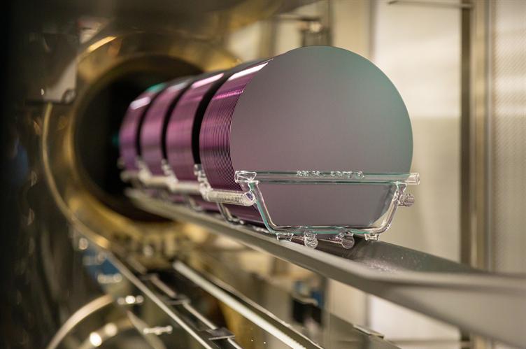
 A Soitec engineer in a clean room. Silicon substrates are being extended beyond the smartphone and into new consumer electronics sectors like smart glasses to drive adoption. Source: Christophe LePetit/Soitec
Swiss army knife of substrates
That’s where fully depleted silicon-on-insulator (FDSOI) technology comes in.
Babureck called FDSOI a “Swiss army knife” platform for semiconductor designers. The technology enables chips to adjust power consumption while supporting a range of integrated functions.
“You can embed memory, RF functionality and even a neural processing unit,” Babureck said. “It’s really a platform designed for ultra-low-power applications.”
And some early smart glasses used this approach. NXP Semiconductors developed an FDSOI-based applications processor aimed at wearable devices and Meta is exploring similar architectures, Babureck said.
FDSOI is also finding its way into optics and sensors. Near-infrared sensors used in facial recognition use this substrate to improve signal-to-noise ratios allowing these chips to detect weak optical signals.
Photonics-based substrates are also gaining traction. Here, the thin silicon layer of the wafer acts as a waveguide to allow the transmission of light signals through chip structures. These substrates are also beginning to appear in sensing and display components for consumer electronics, Babureck said.
Another material potentially of use in the supply chain is silicon carbide (SiC) that can also be used in optical waveguides and display systems, specifically for augmented/mixed reality.
“Leadership in optical-grade silicon carbide today is in China,” Babureck said. “If U.S. developers want a China-free supply chain, they may need to redirect sourcing.”
Pricing is king
While semiconductor manufacturing progress will help smart glasses to reach mass adoption, challenges remain.
Namely, price is still king.
According to Babureck, today’s smart glasses systems can cost close to $1,000 and the price target for broad adoption is likely between $200 and $400. But this will require major improvements in manufacturing scale and cost.
“Scalability is the key,” Babureck said. “The industry may have the technical solution, but scaling it cost-effectively is the challenge.”
Display technology remains one of the biggest hurdles. MicroLED displays, widely seen as a promising solution for augmented reality devices, still face challenges in yield and scalability.
Babureck said like many consumer technologies, smart glasses are likely to follow an S-curve of adoption, with early prototypes giving way to rapid growth once manufacturing hurdles are overcome.
“We haven’t reached the inflection point yet,” Babureck said.
But new materials engineering will be leaned on as much as transistor scaling with the substrate beneath the chip becoming a new frontier for chip performance.
