Researchers at two universities undertook the latest attempt to develop a monolithic three-dimensional integrated circuit without the use of thru-silicon vias (TSVs), the more common method of building a 3-D IC.
The team of researchers at Stanford University and Taiwan-based National Applied Research Laboratories (NARLabs) produced what they claim is a first—a sequentially processed sub-50nm monolithic 3-D IC with integrated logic/non-volatile memory circuits and SRAM. The non-volatile memory exhibits 500 nanosecond response time and the logic circuits operate at 3 picosecond rates.
The researchers have demonstrated the device using multiple layers of ultrathin-body MOSFET-based circuits interconnected through 300-nm-thick interlayer dielectric. The researchers envision closely stacked monolithic 3-D circuits will yield the bandwidth and low power consumption in vertical signal-to-signal communications, and cost-effective manufacturing for producing future mobile devices.
While TSVs provide higher density and less parasitic load compared to conventional wire-bonding approaches, they require large dimensions and long connect distances and exhibit significant parasitic capacitance compared to typical via/contact in CMOS process.
Thus, TSV technology limits the number of vertical data paths and consequentially the achieved bandwidth.
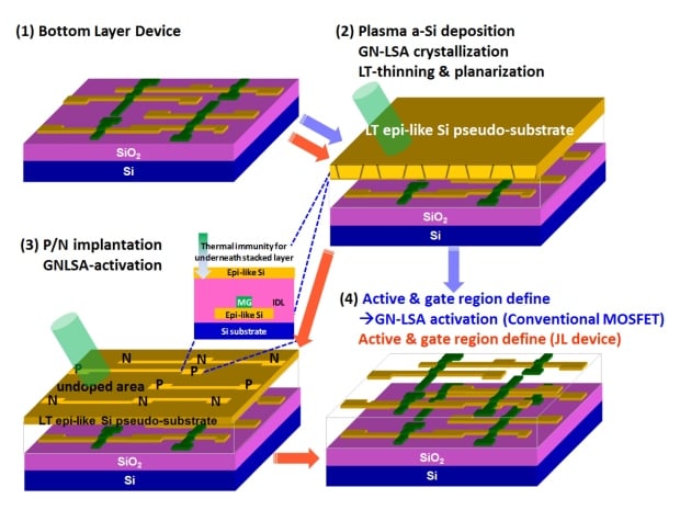
By contrast, 3-D sequential integration (3DSI) approaches achieve higher density in vertical interconnects than TSV technologies by stacking multiple processors, analog circuits, volatile memory and nonvolatile memories in multiple layers with normal vias used in the usual planar CMOS structures.
In a sequentially processed 3-D IC, the interconnects across layers, resembling chip-to-chip TSV bonding, are greatly reduced since the interlayer dielectric is as thin as 300 nm as compared to micron-scaled spacing in TSV-based 3-D IC.
In a technical paper to be delivered at the December International Electron Devices Meeting in Washington D.C., the researchers will detail the 3-D architecture and provide preliminary results showing the power consumption arising from interconnects increasing with scaling.
The 2013 IEDM runs December 9 through 11.
