An ARM Cortex-M0+ microcontroller core that can operate at 250mV is set to be one of the stars of the 2015 International Solid-State Circuits Conference (ISSCC), which takes place in San Francisco, February 22 to 26, 2015.
Although the digital landscape of ISSCC has often focused on the highest performing processors and the largest capacity memories it is clear that energy efficiency has become of at least equal significance. This extends across the "leaf" nodes of the Internet of Things – embedded microcontrollers and multicore system-chip platforms used in smartphones – and up to the high performance engines intended for use in data centers.
If predictions of tens of billions of things connected to the Internet are to become a reality those electronic objects need to lower power consumption by one or two orders of magnitude compared to the state of the art, both in energy per operation and energy consumed retaining state and data.
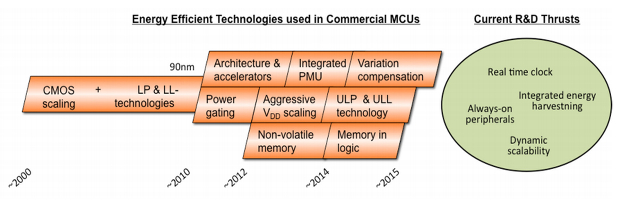
Energy efficiciency techniques exploited in microcontroller design. Source: Stephen Kosonocky, AMD.
Session 8 of ISSCC 2015 is dedicated to circuit implementations of techniques that can help reduce active, leakage and retention power, principally by low voltage operation. Apart from ARM's presentation, other stand-out papers include a near-threshold Cortex-M0+ design from the University of Michigan and a near-threshold SoC that includes a Sparc V8 processor, from STMicroelectronics researchers and implemented using ST's fully-depleted silicon-on-insulator (FDSOI) manufacturing process.
Intel is also showing a focus on low voltage in the same session with a couple of papers outlining voltage regulator circuits that can efficiently drop voltages down to 0.4V and implemented in its 22nm and 14nm FinFET manufacturing processes.
The current state-of-the-art in IoT microcontrollers stands at more than 100-microamps/MHz for full system active power, according to ISSCC sub-committee chair, Stephen Kosonocky, of Advanced Micro Devices.
Therefore ARM's Cortex-M0+-based sub-threshold voltage processor, which can deliver 29kHz clock frequency and 850nW active power at 0.25V should be of great interest (paper 8.1). Implemented in 65nm, 1.2V CMOS the core also enables CPU and SRAM state retention for 80nW power consumption but can scale up to 66MHz clock frequency at 0.9V.
The chip, occupying 1.28 square millimeters, comprises a Cortex-M0+, a low voltage SRAM, a boot ROM, an AES-128 cryptography accelerator and specific communications interfaces. The abstract of the paper claims that the 80nW retention power is one order of magnitude lower than previous sub-threshold designs implemented below 180nm.
With the disclosure within the advanced program of ISSCC 2015, ARM has got some details of its sub-threshold voltage core out slightly before a commercial announcement of the sub-threshold ARM microcontroller family from Ambiq Micro Inc. (see Ambiq Preps Launch of Sub-Threshold ARM MCUs), which that company has dubbed Apollo. As ARM is an investor in Ambiq it will be interesting to see what links, parallels or conflicts there are between Ambiq's sub-threshold microcontroller family and ARM's core.
University of Michigan
And the University of Michigan – where Ambiq founder and CTO Scott Hanson began his research on sub-threshold voltage operation of circuits – also has a Cortex-M0+ presentation at ISSCC 2015 (paper 8.2). The university is presenting what is described as "a battery-less 295pW 1.19mm2 32bit Cortex M0+ processor." There is also a 256 byte SRAM that operates at 0.55V in the circuit.
The circuit is based on an innovation in logic implementation that UoM refers to as dynamic leakage-suppression logic, and which consumes 10fW of active power per gate. The result is that a 0.09 square millimeter solar cell made of bulk silicon can power the core. Clearly a tenth of a square millimeter is tiny so that a larger cell could use to relatively low levels of ambient light to power a microcontroller based on this implementation.
Two more papers in the same session will present the benefits of adaptive voltage scaling (AVS). Texas Instruments (paper 8.3) is scheduled to present a 10.5microamp/MHz 16bit MSP430-based microcontroller at 16MHz in a 90nm flash process. The authors will discuss the use of adaptive body biasing techniques to achieve full state retention of the CPU and SRAM, consuming while consuming just 108nA.
In paper 8.4, ST is due to present a SoC that demonstrates the fitness of its 28nm FDSOI process for near-threshold operation. The SoC is described as a 26pJ/cycle 0.272 square millimeter Sparc V8 processor that operates at 0.45V. This design uses forward body biasing in ST's 28nm FDSOI technology. An AVS scheme is incorporated, comprising a 0.33V/0.45V dual-mode switched-capacitor dc-dc converter, a timing monitoring system, and a 1.51pJ/cycle open-loop clock multiplier.
This and other related topics will be discussed at length at ISSCC 2015, across 27 sessions. ISSCC is scheduled to take place Feb. 22-26, 2015, at the San Francisco Marriott Marquis Hotel.
Related links and articles:
News articles:
Ambiq Preps Launch of Sub-Threshold ARM MCUs
TSMC's Near-Threshold Lead Will Pay Dividend
TSMC Tips Low-Voltage Processes Aimed at Wearables, IoT
