Researchers from the University of Twente in the Netherlands working with semiconductor equipment company SolMateS BV have developed a method to reduce transistor power consumption. SolMateS is a University of Twente spin-off company that specializes in pulsed-laser deposited lead zirconate titanate (PZT) thin-film on top of silicon (PZT-on-Si).
Strain has been used to improve transistor performance in MOS transistors for several nodes, usually through the creation of strain-inducing expitaxial regions adjacent to the transistor channel to improve carrier mobility and transistor performance. Silicon germanium adjacent to the p-channel can produce compressive stress while silicon carbide adjacent to the n-channel transistor produces tensile stress.
However, these stresses are fixed at production and transistors also suffer from current leakage. The MESA+ research institute has proposed that by enveloping the transistor – specifically a FinFET where the channel stands proud of wafer surface – in a shell of piezoelectric material that distorts when a voltage applied, this leakage current can be reduced by a factor of five compared with the same dimensioned transistor without the material.
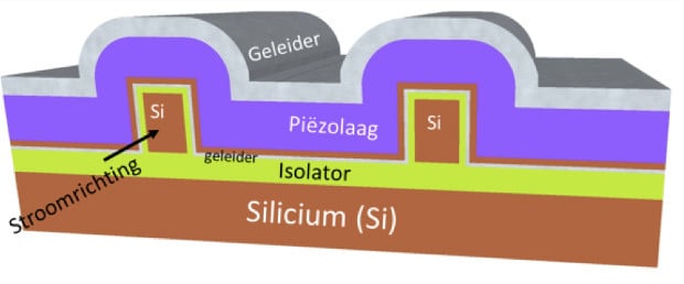
FinFETs are overlayed with conductor and piezoelectric material. The conductors control the amount of mechanical tension, and also the number of electrons in the FinFET channel. Source: University Twente
The piezoelectric material expands when you apply a voltage to it and compresses the silicon in the transistor with a pressure of about 10,000 atmospheres. This high pressure ensures that electrons flow through the transistor faster.
The prototype transistor developed at University Twente is only put under pressure when required and the energy needed to switch the transistor from on to off is thereby partly replaced by mechanical tension. The ability to control the strain electrically means that the transistor can be optimized for current leakage when it is not operating and for energy consumption versus performance when it is active. In the latter case, it is estimated that energy consumption can be reduced by approximately 10 percent.
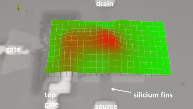
Upward movement of a piezo FET with 5 parallel fins as a result of the piezoelectric effect. When an electrical current is applied across the piezoelectric material, the green parts do not move, but the red ones do. Source: University Twente.
"The design is still fairly crude where the material is concerned. With the further development of the transistor, it should therefore be possible to achieve a further significant increase in efficiency," said Ray Hueting of the MESA+ research group, in a statement. The same research group predicted the operating principle of this transistor in 2013. However, it was with the support from SolMateS that the team was able to insert a buffer layer between the silicon and the piezoelectric layer.
An article presenting the prototype of the transistor appears in the June issue of Transactions on Electron Devices.
Related links and articles:
News articles:
FDSOI: Is Cadence, Not Samsung, the Tipping Point?
