
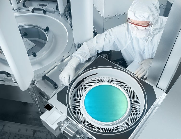
Lam Research plans to invest $3 billion to expand its global R&D lab network, which will include adding infrastructure and capabilities to increase experiment capacity by more than 50%.
The investment will take place over the next five years.
The R&D labs operate integrated 24/7 networks, and the investment will help to compress product development cycles for customers. Lam said the combined R&D infrastructure supports more than 1 million experiments annually that research:
- New chemistries
- New materials
- New mechatronics
The integrated lab network also allows tools, data and more to be shared across locations and time zones in U.S., Asia and Europe. This has allowed Lam Research to shorten process development by up to 2.5 times, the company said.
Why it matters
According to market research firm Yole Group, demand for deposition and etch equipment is expanding rapidly due to AI-related investment.
“Wafer-level semiconductor device processing is the backbone of all semiconductor ecosystems and the enabler of subsequent chip technology advancements,” said John West, chief analyst, semiconductor equipment at Yole Group.
West said etch, deposition and advanced packaging wafer fabrication equipment helps to find the right combination of power consumption, performance, price and form factor for AI semiconductors.
