
The semiconductor industry is reevaluating its long-term roadmap for manufacturing the most advanced chips. High-Numerical Aperture (High-NA) lithography, once seen as the unequivocal path to sub-2 nm node miniaturization, is now being weighed against other options.
Despite its status as a landmark achievement in optics, the significant challenges and immense capital investment required for High-NA have spurred parallel development of complementary patterning techniques. In fact, these technologies are gaining traction as competitive and practical alternatives.
This is not a rejection of optical advancement. This is a pragmatic embrace of a multi-faceted toolkit, in which advancements in materials science, physics and innovative processes converge to overcome formidable barriers.
High-NA, with its $400 million price tag for future node production, represents the world’s most advanced and expensive chipmaking machine. Built by ASML, it promises a compressed wavelength, a wider lens and 8 nm resolution. The higher NA gathers more light to enable finer patterning, but instead of widening the lens it reduces the imaging field.
The latest High-NA scanners can process 220 wafers per hour. Intel Corp. was the first company running High-NA for scaling logic and memory devices but many others are likely coming.
Alongside the pursuit of cutting-edge optical tools, a pragmatic focus is emerging. Engineers are now championing alternatives that prioritize cost-efficiency and manufacturability. This includes eliminating exorbitant cleanroom retrofits, enhancing structural stability, advancing pellicle designs for better light transmission and reducing reliance on intricate wafer-field stitching. Alternative approaches are increasingly recognized as vital, practical solutions for targeted applications within the heterogeneous integration landscape of modern chip design.
Deep ultraviolet’s unlikely revival
Perhaps the most surprising development is the renewed relevance of Deep Ultraviolet (DUV) immersion lithography. Once considered a technology nearing obsolescence, DUV has proven to be indispensable. This longevity is a testament to its process maturity and the vast existing infrastructure that supports it.
Through refinements in multi-patterning techniques, using sequential litho-etch cycles, engineers can now achieve pitches well below the optical resolution limit. This process extracts unprecedented capacity and performance from 193 nm optics, enabling the production of finer features through repeated and precise exposures.
Spacer-based flows, such as self-aligned double patterning (SADP) and self-aligned quadruple patterning (SAQP), subdivide structures into ever-tighter geometries. According to a report from Semiconductor Engineering, these approaches push DUV well beyond its nominal 40 nm half-pitch limit, delivering 20 nm and below through precise overlay control and rigorous inspection.
Within the broader family of etch-based processes, spacer techniques complement pitch splitting methods like litho-etch-litho-etch (LELE), but with fewer design-side complications and proven success in scaling NAND flash and finFET structures. By employing deposition and etch cycles to form sidewall spacers, SADP and SAQP allow chipmakers to reproduce geometries without relying on ever more expensive exposure steps.
At Semiconductor Manufacturing International Corporation (SMIC), independent audits of 7 nm devices confirmed that DUV-only strategies, using aggressive multi-patterning instead of High-NA can deliver fully functional chips. This validation, made clear in TechInsights’ teardown of Huawei’s Kirin 9000S processor, demonstrates that DUV remains capable of producing advanced nodes thought to be reserved exclusively for High-NA.
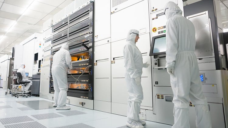 Nanoimprint lithography (NIL) integrated into a 200 mm/300 mm foundry process in an Imec lab. Source: Imec
Nanoimprint: A mechanical paradigm shift
Nanoimprint lithography (NIL) takes a radically different approach from traditional photolithography. In contrast to using light to project an image, NIL physically stamps a pattern into a low viscosity resist using a master template and hardens it through UV light and thermal curing. This direct mechanical transfer completely sidesteps the diffraction limit of light, along with the related issues inherent in optical methods such as photon shot noise and the need for increasingly complex optical proximity correction.
Recent advancements have propelled NIL from laboratory curiosity to a production-ready manufacturing technology. Companies like Canon and, notably, the Chinese firm Prinano, have developed production worthy tools. Prinano’s PL-SR system for 300 mm wafers claims capabilities to imprint features below 10 nm with an overlay precision with less than 2 nm variation. The inherent strengths including dramatically lower tool cost, minimal energy consumption and the absence of cumbersome laser and optical systems make it attractive for high volume, repetitive lithographic techniques.
In specific domains, NIL’s value proposition is most compelling.
- Memory: The regular, dense arrays of NAND flash and DRAM are ideal for a single-step imprint process.
- Photonics and silicon interposers: Fabricate patterns for waveguides and through silicon vias (TSVs).
- Compound semiconductors and novel substrates: Unlike optical lithography, NIL is agnostic to the substrate’s material or topography, enabling fabrication on curved, flexible or non-silicon surfaces.
While challenges in template defectivity, master durability and overlay for complex logic layers remain, NIL has successfully carved out a significant niche. NIL is unlikely to replace High-NA for logic at sub 5 nm nodes, its ascent in adjacent applications creates a parallel scaling roadmap.
Pattern shaping technologies
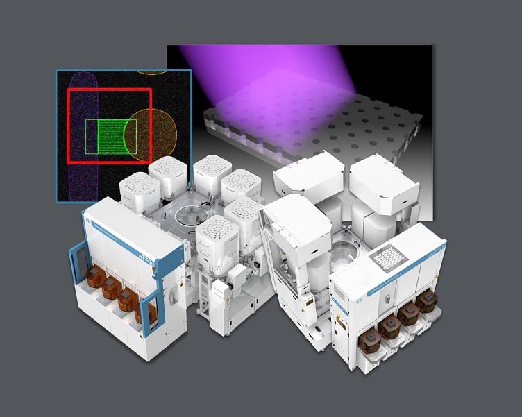
Acknowledging that High-NA lithography is imperfect, there is a new class of processes that correct and refine elements post-exposure. Among these, Applied Materials’ Centura Sculpta introduces geometry shaping, a digital sculpting technique that mitigates the stochastic effects inherent in High-NA lithography while reducing reliance on costly multi-patterning. Sculpta uses directional ribbon beams to elongate printed features, bringing tip-to-tip spacing closer than a single pass can achieve. In addition, it removes bridge defects that otherwise would degrade yield.
Tokyo Electron’s Acrevia system applies gas cluster beam (GCB) technology to reshape and refine patterns after lithography, as well. Following initial exposure and dry-etch, Acrevia directs high energy clusters of gas atoms at controlled wafer angles to adjust sidewall dimensions, smooth rough edges and reduce stochastic effects. By lowering the line edge roughness and correcting within-wafer variation, the tool reduces the need for double exposure layers.
Post-lithography optimization functions as a corrective stage, refining profiles after exposure instead of repeating them. Such systems integrate seamlessly into current High-NA flows, acting as both yield savers and overlay buffers. Furthermore, they provide a crucial counterbalance, reducing the industry's strategic dependence on optical scaling alone.
The hybrid playbook
High-NA is inherently selective, dictated by both physical limits and economic tradeoffs. Its deployment is a strategic engineering choice focused on extraordinary resolution. The result is a paradigm where hybrid patterning optimizes cost, throughput and capability across the full lithographic stack.
In the hybrid model, every tool has its own role. High-NA is used for the most critical front-end layers like fins, gates and contacts. Alternatives become the workhorse, defining key interconnects and logic levels. DUV immersion is used for dense, regular structures such as SRAM bitcells and selected metal layers. NIL finds its niche in photonics and micro-electro-mechanical systems where cost and unique material versatility are transformative. Crucially, this entire multi-tool flow is underpinned by post-patterning feature rectification technologies.
Together, these systems act as a universal corrective measure to improve critical dimension uniformity and relax performance requirements and cost burdens. The hybrid approach demonstrates a fundamental evolution in engineering philosophy, embracing a system-level perspective.
Conclusion
For decades, Moore’s Law guided the industry with a predictable formula: Smaller transistors, faster chips and cheaper performance. High-NA emerged as its intended continuation, the optical marvel designed to extend scaling into the sub 2 nm era. Today, that vision persists but in a changed context.
Mature technologies can reinvent themselves. Moore’s Law bends. Engineers still pursue density but through a mosaic of optical, mechanical and chemical processes. High-NA may retain its place at the top, yet its dominance is tempered by alternatives that carry equal weight in chipmaking.
This strategic expansion opens a new era of semiconductor miniaturization. Coming innovations will hinge less on a single breakthrough and more on the strategic coordination of multiple methods, each tailored to specific needs. What follows is a more holistic framework where economic viability, manufacturability and fundamental physics share equal authority in guiding semiconductor engineering progress.
