
ROHM has developed a 30 V N-channel metal-oxide semiconductor field-effect transistor (MOSFET) — AW2K21 — in a common-source configuration that achieves an industry-leading ON-resistance of 2.0 mΩ (typ.) in a compact 2.0 mm × 2.0 mm package.
With the rise of compact devices featuring large-capacity batteries, such as smartphones, the need for fast charging functionality to shorten charging times continues to grow. These applications require bidirectional protection to prevent reverse current flow to peripheral ICs and other components when not actively supplying or receiving power. What’s more, fast charging involves high current power transfer, leading smartphone manufacturers to demand stringent specifications for MOSFETs, including a maximum current rating of 20 A, breakdown voltage between 28 V and 30 V, and an ON-resistance of 5 mΩ or less. However, meeting these requirements with standard solutions typically necessitates the use of two large low ON-resistance MOSFETs, increasing board space along with mounting complexity. 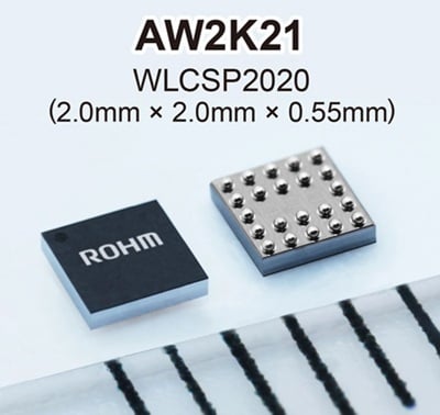 Source: ROHM
In response, ROHM developed an ultra-compact low ON-resistance MOSFET optimized for fast high-power charging. The AW2K21 adopts a proprietary structure that enhances cell density while minimizing the ON-resistance per unit chip area. Two MOSFETs are integrated into a single package, allowing a single part to support bidirectional protection applications (commonly required in power supply and charging circuits).
The proprietary structure also places the drain terminal on the top surface, unlike on the backside in standard vertical trench MOS structures. This enables the use of a WLCSP, which achieves a larger chip-to-package area ratio that further reduces ON-resistance per unit area. As a result, the new product not only minimizes power loss but also supports high current operation, making it ideal for high-power fast charging applications despite its ultra-compact size.
For example, in power supply and charging circuits for compact devices, standard solutions typically require two 3.3 mm × 3.3 mm MOSFETs. In contrast, the AW2K21 can achieve the same functionality with a single 2.0 mm × 2.0 mm unit, reducing the footprint and ON-resistance by approximately 81% and 33%, respectively. Even compared to similarly sized gallium nitride (GaN) high-electron-mobility transistors (HEMTs), ON-resistance is decreased by up to 50%, contributing to lower power consumption and increased space savings across a variety of applications.
The AW2K21 is also suitable for use as a unidirectional protection MOSFET in load switch applications, where it maintains the industry’s lowest ON-resistance. At the same time, ROHM is further pushing the limits of miniaturization with the development of an even smaller 1.2 mm × 1.2 mm model.
Going forward, ROHM remains dedicated to supporting the miniaturization and energy efficiency of electronic systems through compact, high-performance solutions that contribute to the realization of a sustainable society.
