Around 2019, semiconductor manufacturers started marketing their SiC and GaN product portfolios as options for high-frequency designs, high-power designs, or systems with both capabilities. GaN and SiC components were originally targeting applications such as high-power conversion and 5G infrastructure. To date, SiC and GaN have seen significant adoption in high power conversion and high current battery charging applications, largely driven by electric vehicles and their required charging architecture.
One implementation of the two materials in RF power amplifiers is as a stack, known as GaN-on-SiC, which was intended to give the high-power handling benefits of SiC and the high-frequency operation of GaN in a single component. However, silicon may make a comeback in this application area as the substrate for a GaN-based amplifier, known as GaN-on-Si.
Due to the high-frequency characteristics of GaN, it is likely that GaN-on-Si will be the next material set to dominate the RF power amplifier market. This platform overcomes the existing limitations of GaAs in terms of frequency range and power handling and leverages an existing technology with an extensive supply chain. This will contribute to cost reduction and yield maximization of GaN-on-Si amplifiers, and it may enable a new generation of highly integrated RF components.
What can you do with GaN-on-Si?
GaN is one compound semiconductor that offers superior performance over silicon and SiC in two areas that are very important for power electronics and RF:
- Faster switching speed due to high electron mobility
- Higher bulk thermal conductivity
These two specifications are both very important in power electronics. With faster switching speeds, GaN FETs used in switching regulators will exhibit faster edge transitions when driven with a pulse train, which reduces switching losses during operation. This also allows pushing the limits on certain types of power converter designs (bridges and push-pull), which can exhibit shoot-through as a driving PWM pulse train’s duty cycle nears 50%.
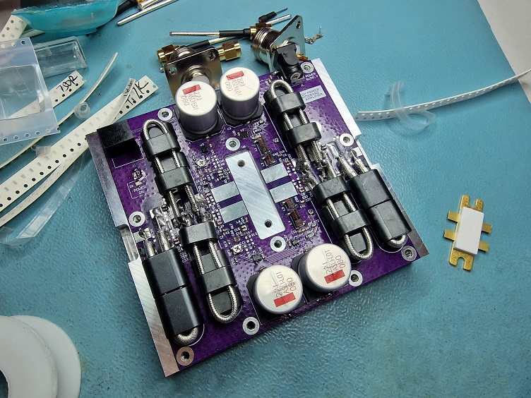
In terms of device design, GaN components are normally fabricated on another semiconductor wafer (either silicon or SiC), although pure GaN wafers are available. Both GaN-SiC and GaN-on-Si involve epitaxial deposition of GaN on a silicon wafer, followed by circuit patterning and formation of active device areas, such as in the GaN HEMT shown below.
 A finished 200 mm GaN-on-Si wafer that will be used for power amplifiers and 5G infrastructure. Source: MIT
This structure can also be bonded to devices on a Si CMOS wafer with the oxide layer as the bonding interface, forming a device with GaN circuitry integrated with standard Si CMOS devices. This is a powerful combination that brings CMOS circuits (logic, analog circuits, etc.) into the same package as a GaN-based device. This level of integration enables higher power densities compared to silicon devices with RF and digital capabilities.
GaN-on-Si compared
The ability of GaN/GaN-on-Si FETs to switch faster than silicon FETs also ensures lower losses in AC operation, even when driven with signals in the GHz frequency range. The safe power and frequency operating regions for GaN devices in comparison to SiC devices is shown in the graph below.
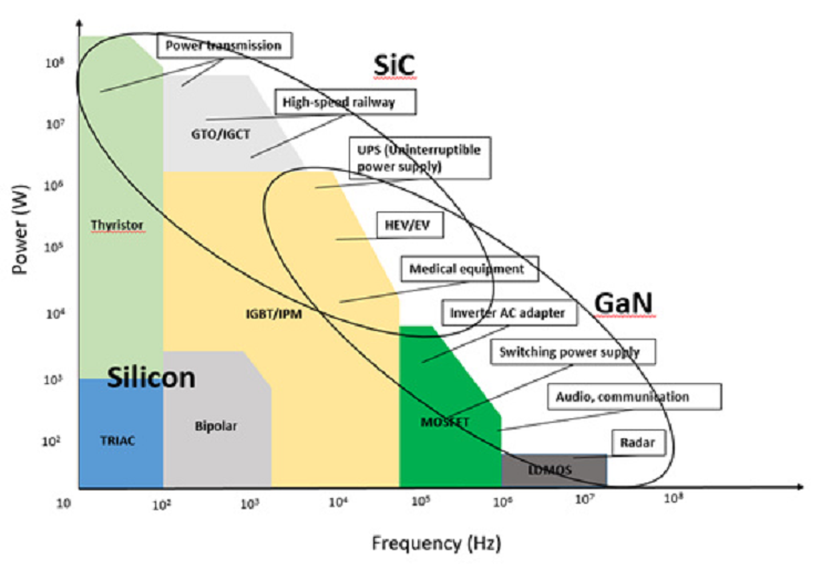 Comparison between silicon, GaN and SiC semiconductor devices and their target applications. Source: Rogers Corp.
The graphic below shows a similar performance view but looking at materials capabilities more generally. Note the comparison between GaN-on-Si and GaN-SiC.
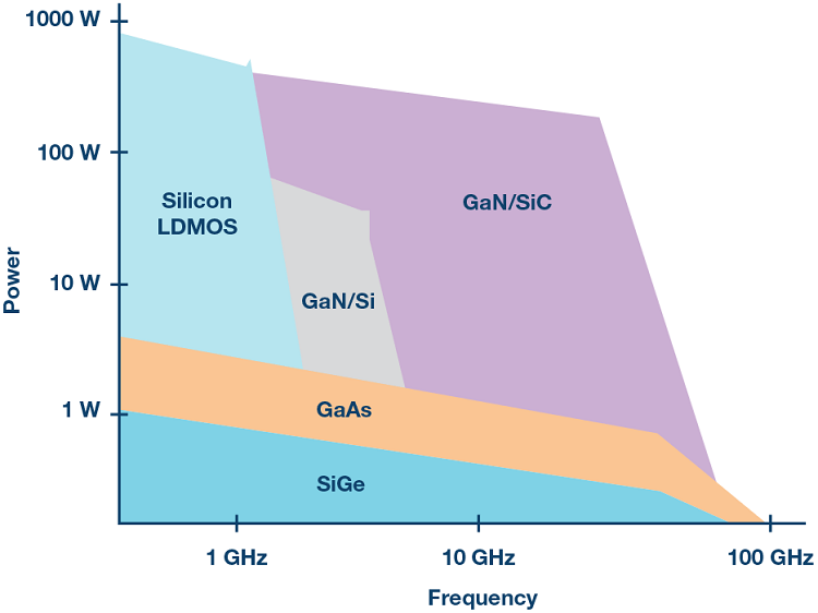 This graph shows a comparison of GaN-on-Si against other semiconductors for RF power amplifiers. Source: Analog Devices
From the above performance regions, it should be clear what makes GaN so attractive as a material platform for RF semiconductors and power electronics: these designs can handle similar power levels at higher frequencies compared to SiC, Si and GaAs. From the device perspective, specifically looking at GaN HEMT devices, GaN-on-Si and GaN-SiC easily outperforms pure silicon and SiC devices.
With GaN and SiC both offering an edge over silicon in terms of power and operating frequency, GaN-SiC initially appeared to be an attractive option for device fabrication. Using SiC as the substrate for a device would eliminate an expensive GaN wafer, which would reduce the cost of an advanced RF/power device while also getting a performance edge over silicon. However, when we look at the cost, yield and capabilities together, leveraging the existing silicon supply chain makes the most sense.
Extensive silicon supply chain
The most compelling reason GaN-on-Si is poised to take over the RF power amplifier market is due to the extensive existing supply chain for silicon. 200 mm silicon wafers can be used as a platform for GaN growth while also integrating with Si CMOS, as outlined above; leveraging these mature silicon-based technologies gives multiple advantages for GaN-on-Si as a material for RF power amplifiers:
- Rapid availability of Si production capacity reduces cost compared to pure GaN and GaN-SiC.
- Extensive processing experience ensures high yield and leverages existing equipment.
- Silicon has a thermal conductivity value that is comparable to SiC, which ensures reliability at high power.
- Integration of Si CMOS onto GaN-on-Si brings logic and other functions into the same device with high-frequency/high-power components.
Due to these factors relating to performance and supply chain dynamics, it is easy to conclude that GaN-on-Si is the optimal choice for RF power amplifiers. While GaN-on-SiC provides similar power levels at higher frequencies, this is overkill for today’s wireless devices, and the extra cost involved means that GaN-SiC does not provide any additional advantages.
