ZEISS announces the new ZEISS Crossbeam 550 Samplefab, a focused ion beam scanning electron microscope (FIB-SEM) optimized for fully automated preparation of transmission electron microscopy (TEM) samples (lamellae). Built for efficiency and throughput in the semiconductor lab, ZEISS Crossbeam 550 Samplefab provides recipe-based automation for the routine TEM sample preparation work of bulk milling, lift-out and thinning at any number of target points on the sample. The solution promises an automation yield of greater than 90% for processing lamellae from bulk to TEM grid without operator intervention. Automated checks allow human interventions to ensure no lamellae are lost during processing, driving lamella success rates toward 100%.
TEM imaging provides essential information for understanding semiconductor device defects and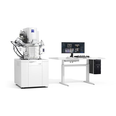 Source: ZEISS improving process yield. However, the accuracy of the data from TEM analysis is dependent upon producing high-quality lamellae accurately, repeatedly and with high throughput.
“To address the growing industry need for TEM sample preparation, we have built a dedicated FIB-SEM, the ZEISS Crossbeam 550 Samplefab. Our focus is to offer the most robust automation available on the market today, allowing fully unsupervised operation of down to 100 nm thin lamellae with high accuracy and throughput,” said Dr. Thomas Rodgers, head of business sector electronics at ZEISS Microscopy. “The system’s user interface is completely new, designed for a rapid learning curve and intuitive operation by both novices and experts. With the new Crossbeam 550 Samplefab, customers can automatically process ten lamellae in under eight hours, starting from a bulk sample and ending with a thinned lamella ready for the TEM.”
ZEISS Crossbeam 550 Samplefab uses the Gemini 2 electron column, allowing the operator to observe the sample live with the SEM during FIB milling to achieve the highest final lamella quality and endpointing outcomes when thinner samples are required than what is provided by the automation.
“Our FIB column is extremely stable, and while we have an automated calibration routine, users report rarely needing to calibrate or align the system over multiple weeks, especially if it is working on routine processes. This dramatically reduces the operator effort, and the time spent setting up the tool prior to an automated run,” said Rodgers. “What’s more, the workflow is so robust that dozens of lamellae can be created using a single probe tip, which only needs reshaping after a few days of heavy use. The tip can be sharpened with a simple reshaping operation that takes less than 30 minutes, and the needle can be reshaped multiple times before needing to be replaced; a new tip exchange takes only half an hour. This dramatically increases the productive uptime of the tool, and lowers the cost spent on consumables.”
