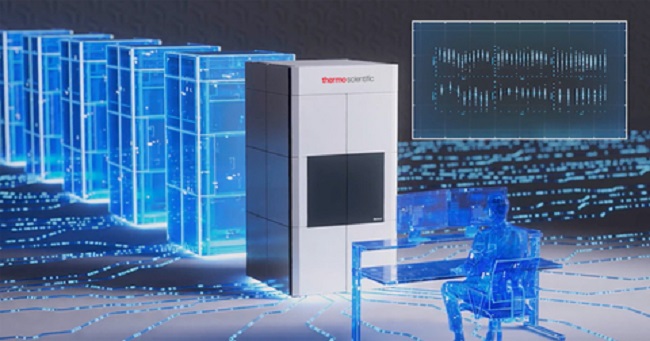
A fully automated scanning transmission electron microscope ((S)TEM) metrology solution has been designed by Thermo Fisher Scientific to help enhance productivity and deliver data quality assurance for high-volume semiconductor manufacturing.
The increasing complexity of semiconductor device 3D architectures mandates development of more exact in-depth metrology and characterization processes. The atomic-scale 3D intricacies in emergent devices are driving a need for a highly automated (S)TEM platform to enable faster access to large-volume, high-quality data and help accelerate learning cycles.
Engineered to facilitate yield improvements and reduce time-to-market, the Metrios 6 (S)TEM incorporates advanced hardware and machine-learning algorithms to obtain large-volume high-quality data from complex devices and novel materials rapidly. The system enables fully automated transmission electron microscope metrology and characterization workflows with up to 20% in average productivity improvement compared to the previous Metrios iterations.
 Source: Thermo Fisher Scientific
The system features Smart Stage fully automated sample insertion and retraction mechanism to eliminate manual operation and potential for human errors, enabling users to perform high-resolution imaging at a faster pace. A new Thermo Scientific Ultra-X energy-dispersive X-ray spectroscopy (EDS) detection system also offers fast compositional characterization and elemental mapping to ease challenging analysis on the most beam-sensitive materials and enable at least two times faster data collection.
In addition, machine-learning-enabled automation eliminates tedious recipe generation for routine (S)TEM analysis and provides automated workflows with flexibility to generate large volume data without using highly skilled operators.
