Thermo Fisher Scientific has launched a fully automated wafer analysis system designed to increase productivity in fabs by speeding up how engineers see and understand what’s happening deep inside a semiconductor.
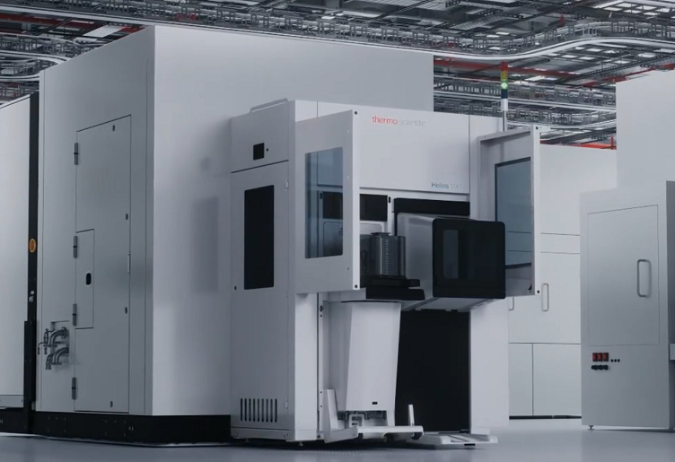
Called the Helios MX1 plasma focused ion beam (PFIB) scanning electron microscope (SEM), the tool uses 3D reconstruction and metrology to enhance analysis of semiconductor logic, memory and packaging devices. This allows engineers to visualize and analyze buried chip structures in fabs.
Helios MX1 shows details that were only previously achievable in a lab, which will accelerate time-to-yield by revealing semiconductor subsurface defects, the company said.
This is needed due to smartphones, autonomous vehicles, supercomputers and more depending on more complicated structures at an atomic scale inside silicon chips, Thermo Fisher said. With these semiconductors increasing in processing power and decreasing in size, any faults can cause massive delays.
“The semiconductor industry is witnessing a dramatic increase in the amount of analysis needed within fabrication environments, and traditional methods are no longer sufficient,” said Mohan Iyer, semiconductor vice president and general manager at Thermo Fisher Scientific. “With Helios MX1, our customers can now have a detailed, three-dimensional look at structures that are beneath the wafer surface.”
