
Advanced packaging of semiconductors is offering opportunities to overcome memory access roadblocks that inhibit high-compute applications. Technologies operating in the data center and at the edge, like AI and vision, have huge memory and compute requirements associated with them, and the latency and density of memory are both challenges that can be solved at the packaging level.
To overcome these challenges, semiconductor packaging designers have followed the heterogeneous integration route to include more memory closer to the processor.
High-bandwidth memory offers solutions to the memory roadblock problems currently confronted in modern processors and embedded systems. These memories provide two advantages for systems designers:
- Reduced component footprint and external memory requirements
- Faster memory access time and rate
Thanks to these advantages, expect to see many more advanced processors include greater amounts of high-bandwidth memory in packages and on modules.
Why include in-package memory?
Look at standard component datasheets (e.g., microcontrollers and MPUs) and computer/server CPUs, and you’ll find plenty of components with on-die/in-package memory. Many different memories have been used in component packages, with Flash being the most common. It’s common to see moderately sized Flash blocks on-chip or in-package used to store small binaries or configuration settings for an embedded application. There may also be small amounts of synchronous random access memory (SRAM) or dynamic random access memory (DRAM) in older packages; many popular microcontrollers include SRAM on-chip as a standard feature.
Therefore, in order to increase memory capacity in high-compute systems, semiconductor manufacturers are including 3D-stacked DRAM chiplets alongside processor core silicon in their CPU packages. Just last year (2022), AMD shipped the first server CPUs with stacked DRAM and SRAM dies in the products targeting data center infrastructure. As more companies perfect the technology, more products are expected to include these DRAM stacks, which communicate with the core through a high-bandwidth memory (HBM) interface.
Stack DRAM structure and performance
The image below shows a typical stacked DRAM structure in a typical heterogeneously integrated package. The stack DRAMs sit on a substrate/interposer stack, where lines are wired to the CPU through to provide the required memory interface. These DRAM dice are connected with vertical through-silicon vias (TSVs) to provide the required connections back to the interposer and, ultimately, to the core.
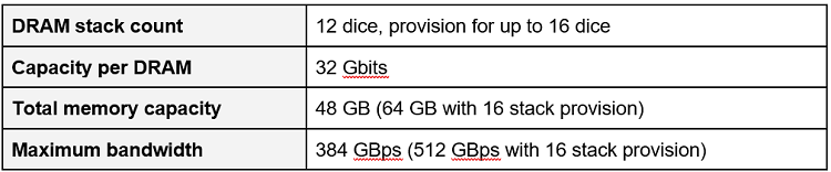
Currently, the HBM3 standard, published by JEDEC, is the governing standard on HBM structural properties and performance. Some provisions in the HBM3 standard are summarized below.
The technology used to build DRAM stacks was originally developed for graphics processors, and yet it has spread to memories to enable the very high bandwidths shown in the above table.
Comparison with other JEDEC RAM types
In total, JEDEC defines three other types of RAM that are different from HBM and appear external to the processor package:
- Double data rate (DDR) — standard RAM used in computers, laptops
- Graphics DDR (GDDR) — used for on-board memory in GPUs
- Low-power DDR (LPDDR) — used primarily in mobile devices (phones, tablets)
Recent trends have continued to push these newer generations of RAM to faster clock speeds so that data transfer rates can be continuously increased. The challenge in prior generations of these memories is that this was the only way to get to high data transfer rates because the bus widths were very narrow. This is not the case with HBM; the bus width in HBM is very wide, so the memory interface can run at a slower rate and yet still provide extremely fast data transfer on a wide bus. This is one of the main operational factors distinguishing HBM from other DDRs.
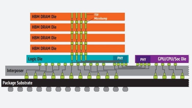 An example of a HBM DRAM stack. Source: AMD
Benefits for systems designers
Embedded systems designers, embedded compute module designers, packaging designers and a host of other designers in related fields gain plenty of benefits from processors with HBM. The biggest benefit is reduction in system size through elimination of external memory chips from the main board. Currently the costs for 3D stacked DRAMs is quite high, but as a marketplace develops for these components and processes advance, expect prices to become more competitive with standard RAM options.
The other benefit to placing memory modules in the package is the reduced time required for high-compute processing operations. This is a major factor that inhibits real-time processing of large datasets in areas such as vision. Each time data has to be fetched from external memory, the processing time increases. Placing processing and memory in the same package eliminates this roadblock and enables much faster compute.
Some contemporary systems that will need these types of components outside the data center include:
- Robotics
- Advanced ADAS
- Imaging radar
- Sensor fusion with vision
- High-performance computing
Of this list of five application areas, systems targeting the first four areas are being built for real-time systems, which require the extremely low processing latencies that could be provided by HBM.
