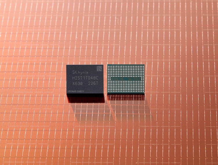
SK Hynix has started sampling its 238-layer 512 Gb triple level cell (TLC) 4D NAND flash memory chips.
The rollout follows the development of a 176-layer NAND product two years ago and SK Hynix calls the development of the 238-layer flash the most layers and smallest cell area at the same time.
The goal is to introduce products that outperform existing ubiquitous 3D products and 4D products have a smaller cell area per unit compared to 3D, which leads to higher production efficiency.
Other features of the 238-layer NAND flash include:
- Data transfer speed of 2.4 Gb/s, a 50% increase from the previous generation.
- Energy consumption on data reading decreased by 21%.
- 34% increase in chip density per unit area.
SK Hynix said the NAND flash will likely be adopted for client and enterprise-based solid state drives (SSDs) before being used for smart devices such as mobile handsets and then other SSDs for consumer use.
The company plans to introduce a 238-layer in 1 terabit capacity in the next year, which is doubling the density compared to 512 Gb products.
