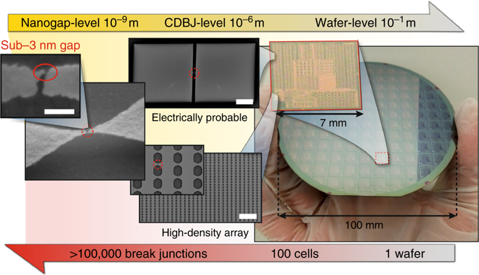
 Hierarchical depiction of the fabrication of crack-defined break junctions on a wafer scale. Source: KTH Royal Institute of Technology
Scalable fabrication of the nanoscale electrodes needed to explore molecules and exploit their behavior as potentially valuable electronic materials is now possible with technology developed by an international research team. The technique yields millions of viable nanoscale molecular junctions -- extremely small pairs of electrodes separated by a nanometer-sized gap where molecules can be trapped and probed -- and could lead to structures that enable single-molecule electronic devices.
Photolithography is applied to pattern a stack of gold on titanium nitride (TiN), which is then set on a silicon wafer. The notched structures that are formed then concentrate stress, and when the silicon directly underneath the stack is removed by release etching, tiny cracks form at the pre-determined locations in the TiN to release the stress. This in turn deforms the gold, stretching it into atomically thin wires running across these cracks, which upon breaking forms gaps as small as a molecule.
The approach produces as many as 20 million electrodes in a five-hour interval, based on the use of a 100 mm diameter wafer of thin materials and placement of gold film on top of a brittle material that forms the cracks. The researchers trapped and studied dithiol-terminated oligo (phenylene ethynylene), a commonly used reference molecule, in the nanometer-wide space between the electrodes to ensure that the fabrication method didn't hinder the formation of molecular junctions.
The goal is to produce gaps that enable a phenomenon called tunneling, in which electrons overcome the break in a circuit. A break junction has a gap the size of a few atoms, which breaks the flow of electrons through it, but electrons with sufficient energy can still jump across. Tunneling electrons sustain a small but measurable current that is extremely sensitive to the size of the gap, and to the presence of nano-objects inside it.
Scientists from KTH Royal Institute of Technology in Sweden and Delft University of Technology in the Netherlands participated in this research, which is published in Nature Communications.
